RF power amplifier design
While many electronics textbooks have a chapter devoted to RF
power amplifiers, and also several complete books about this matter
exist, I haven't yet found any that explains the whole topic in a way
that would enable an electronics hobbyist, or even a practically minded
professional circuit designer, to fully understand the matter and
achieve designs that work well and for a long time. Most books treat
this matter in a totally theoretical way, with excessive use of maths.
Practically-minded electronicians most commonly don't understand the
sort of mathematical language used in those books, while the
mathematicians and theoretically minded engineers who do understand
them are usually not the people who would actually design and build an
amplifier!
Many people have asked me to write an article about RF power
amplifiers, in a way that practical electronicians can understand. Also
over
many years I have come to acquire a better understanding of these
circuits, which often work in ways that are far less trivial than their
schematics look. Now, in 2020, confined at home due to the COVID-19 pandemic, time
has
come to write this article.
Most books about RF power amplifiers are mainly oriented
toward the cellphone market, so they place a big emphasis on UHF and
microwave amplifiers, often not even mentioning HF. For this reason I
will aim my article mainly at HF, extendable to VHF. In fact, as a
long-time radio amateur, I have ham radio applications in mind as my
primary
design objects. So this article is oriented mainly at power amplifiers
operating in the range of 1.8 to 54MHz, sometimes to 148MHz, in a power
range up to 1500W. I will include driver stage design down to the
milliwatt level.
This is a very long web page, almost long enough to be printed in book
form, and if you are really interested in the
matter, you will need to work through it step by step. It's organized
by background color: The main article has my traditional yellow
background, while accessory explanations are on blue background. If
you already know what I explain in such a Blue Block, you can skip
right over it and continue reading the main article.
I will consider the specific quirks of both BJTs and MOSFETs. Since
MOSFETs are far more common nowadays, I will draw MOSFETs in
all those situations that are applicable to both types of transistors.
Throughout this article, when I write "transistor" it means that
the matter described is applicable to both types, and I will talk about
source, drain and gate as a matter of standards, even when that could
be emitter, collector and base. When I write "BJT"
and "MOSFET" it means that the matter is specific to one type.
Totally obsolete devices, like vacuum tubes, aren't considered. And
YES, in
2020 tubes are indeed totally and fully obsolete, in the power and
frequency ranges considered in this article! So don't be mad at me, and
try not to shed any tears over this fact. Even BJTs are
basically obsolete at this time for RF power use, and most are no
longer being manufactured, but there is still a lot of equipment around
that
uses BJTs, so I'm including them.
Classes
of amplifiers:
In
the beginning of electronics, shortly after Adam invented the vacuum
tube and Eve promptly criticized him for doing so, amplifiers were
divided into three
main
classes. Any amplifier in which the active device
conducted current all the time, throughout the entire signal
waveform, was called "class A". Any amplifier in which the active
device conducted current during exactly one half of the driving
signal's waveform, usually the positive half, was called "class B". And
any amplifier in which the active device conducted current during less
than one half the driving waveform was called "class C".
Soon
after doing this classification, the Adam of electronics noticed that
he had forgotten to consider all those amplifiers in which the active
device
conducts current during more than half of the signal's waveform, but
less than the whole time. Since this mode of operation falls between
class A and class B, and given that despite much desperate searching no
letter
could be found between those two, this operation mode was called "class
AB".
Electronicians
love to talk in angles. So the whole period of an RF cycle is
considered to have 360 degrees. For this reason one can say that
transistors operating in class A conduct over 360°, while in
class AB they conduct during less than 360° but more than 180°, in
class B they conduct exactly during 180°, and in class C they conduct
for less than 180° of the signal's period.
Since it
is very hard, or even impossible, to bias a transistor precisely to its
conduction threshold (which by the way is poorly defined!), so that it
conducts exactly
for 180°,
true class B amplifiers strictly don't exist! For that reason some
designers use the "class B" designation for any amplifiers that are close to true class
B, that is, amplifiers that operate in class AB but with a very small
idling current, so that they conduct for just slightly more than 180°.
I will call such amplifiers class AB, but if you read certain textbooks
and papers you need to know that my class AB could be called class B by
some authors.
A
theoretically perfect amplifier, using perfect components, would
achieve a maximum efficiency of 50% in class A and 78.5% in class B,
both at the limit of starting to cause distortion by clipping the
signal. A class C amplifier
has higher efficiency than that. The smaller its conduction angle is,
the
higher is its efficiency, but the lower is its output power. As the
conduction angle approaches zero, the efficiency approaches 100%, but
the power output approaches zero, so that's not very useful.
It is
often said that class A, AB and B amplifiers are linear, while class C
amplifiers are not. But this is incorrect! Firstly, all amplifiers have
residual nonlinearities that cannot be fully eliminated. Secondly, an
A, AB or B amplifier will turn dramatically nonlinear when overdriven,
and sometimes they are deliberately operated in this overdriven,
nonlinear mode.
And thirdly, and this is a point many people haven't realized, a class
C amplifier can be built to be linear! All it takes is devising a
biasing scheme that keeps the class C amplifier operating over a constant conduction
angle, even while the amplitude varies. But this
technique is rarely applied, so in practice most class C amplifiers are
indeed nonlinear.
Long
after Adam had ceased doing electronics, more amplifier classes were
added, and these aren't based on conduction angle. And they are
usually
more efficient than the old ones. In class D amplifiers the transistors
are switched on and off, instead of being linearly driven. There are
two ways to implement a class D amplifier. In one of them the
transistors switch the output voltage,
which then attains a nearly square waveform, while the output current
is
defined
by the resonant circuit coming after the transistors, and is roughly
sinusoidal. In the other kind, the transistors switch the output current, resulting
in a nearly square current waveform, while the resonant circuit at
the output defines the voltage waveform, which becomes nearly
sinusoidal. The two types are called, appropriately, "voltage-switching
class D", and "current-switching class D" amplifiers.
In class
E amplifiers the transistors are also switched on and off, but a
resonant output network is used that shapes both the current and
voltage waveforms to be non-square, and this largely avoids
simultaneous voltage and current on the transistor, further improving
efficiency. If a transistor actually could be switched
instantaneously, class E wouldn't be necessary, as class D would be
perfect - but real transistors can't switch that fast. Class E
amplifiers basically work by the tuned output network largely
lifting the instantaneous load on the transistor during the
non-zero duration switching transitions, which enables getting very
high efficiency from relatively slow transistors.
Class F
amplifiers also use transistors in switching mode, but use a more
complex output network that treats the odd harmonics in one way, and
the even ones in another. This results in voltage and current waveforms
that optimize both the efficiency and the achievable power output, for
a given transistor.
In addition to these 7 basic amplifier classes, there are several more,
which have been defined by specific designers and companies, and
are often treated as intellectual property by them. Two different
companies might assign different class letters to basically the same
amplifier type.
It should be noted that the definitions of the classic classes A to C,
and the
new kids D to F, overlap, because the classic ones are defined by
conduction
angle, and the modern ones by circuit layout and waveforms. Transistors
in class D, E and F amplifiers theoretically operate with 50% on, 50%
off time, and thus would be considered class B amplifiers by the old
definition, driven into saturation. But often in practice their
conduction angle is slightly different from 50%, and thus they
become either class C or class AB amplifiers by the old
definition. This is important to bear in mind, because many transistor
datasheets give circuit examples which the manufacturers claim to
operate in class AB, but that truly are operating in class D. The power
output and efficiency claimed by the manufacturers is very high,
typical for class D,
but people reading the datasheets and noticing the "class AB" claim
will mistakenly believe that the transistor described can deliver that
high
power and efficiency while operating linearly! This has led many ham experimenters to
blowing up expensive MOSFETs by operating them at unrealistically high
power levels in linear class AB, trying to achieve the same power that
the manufacturer claims for the nonlinear class AB / class D
hybrid test circuit.
RF power
amplifiers are best designed backwards. that is, you start
at the output side, and then continue toward the input side. When
designing a multistage amplifer, you start with the final stage, then
continue to the driver. Keeping with this logic, let's start looking at
output circuits for various types of amplifiers.
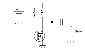
Single-transistor broadband amplifiers:
This kind of amplifier is usually operated in class A. There
is a constant supply current flowing through a choke. The
transistor conducts more or less of this current to ground, as
commanded by the drive signal. The remainder of the current is forced
to go through the load resistance. A coupling capacitor
allows the RF current to flow, while blocking the supply voltage.
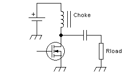
In all circuits on this page, the battery represents a perfect, stable
voltage source. In a practical amplifier there wouldn't be a real
battery, of course, but a combination of bypass capacitors, typically
fed from a regulated power supply, sometimes through an
additional choke. And the gate, drawn open
here, obviously needs to be connected to a circuit that applies a DC
bias and an RF drive voltage.
Since a choke cannot have any DC voltage across it, the supply
voltage appears in full at the drain of the transistor. When the
transistor is
driven harder during the positive half cycle, it conducts more current
and thus temporarily pulls its drain voltage down. The additional
current flowing
in the transistor at that time comes from the capacitor, thus drawing a
negative current through the load resistor. Likewise, when the
transistor is being driven softer, during the negative half of the
driving waveform, it conducts less current than what's coming through
the choke, and the surplus must flow through the capacitor and
resistor. That's a positive current in the load resistor, and the
voltage at the drain becomes higher than the supply voltage.
In normal
operation, a typical RF power transistor can pull its drain voltage down to
about one tenth of the supply voltage. If the drive signal is
symmetric, and the transistor is linear and all
goes as it should, then the output signal will also be symmetric,
undistorted, and will reach a peak value equal to 90% of the supply
voltage. Thus the peak-to-peak
output voltage can reach 1.8 times the supply voltage, and since RMS
voltage is the peak-to-peak value divided by 2√2, that's an
RMS voltage of about 0.64 times the supply voltage. This is the
maximum effective undistorted RMS voltage that can appear on the load.
And since power is RMS voltage squared and then divided by load
resistance, it's easy to calculate the power available on the load. For
example, if the supply provides 12V, and the load resistor is 10Ω, then
we get 21.6Vp-p on the load, which is roughly 7.6Vrms, and on 10Ω that
makes roughly 5.8W. Note that the exact value depends on the actual
saturation voltage of the transistor, which changes according to
transistor type and operating conditions. The 10% saturation voltage I
assumed here is
typical, but individual situations can stray considerably from this
value.
The DC current in the choke will be determined by the transistor's
biasing. To obtain correct, undistorted operation, it's necessary that
the transistor never runs out of drain current, and thus it has to be
biased
to a DC current larger than the peak signal current. That's class A
operation. Since this peak signal current is roughly 0.9 times the
supply voltage divided by the load resistance, in the example above it
is 1.08A, and you would probably fare well by biasing this transistor
to some DC value between 1.2 and 1.5A.
If you need a different output power, and the supply voltage is given,
then the only item you can adjust to suit that requirement is the load
resistance. But typically there is a requirement to make the amplifier
work into a specific
load resistance too! So it's most usual that some transformation of the
load resistance is required. This could be done by means of a
transformer inserted between the amplifier and the load, like this:
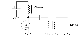
The transformer can be of the conventional type, as shown in this
drawing, or it could be a transmission line transformer. In a
conventional transformer, the turns ratio is equal to the
voltage ratio, inversely proportional to the current ratio, and
equal to the square root of the resistance or impedance ratio. For
this reason it's important to always make sure you understand whether a
transformer said to have a certain ratio, such as 1:4, is meant to have
a turns ratio and voltage ratio of 1:4, or an impedance ratio of 1:4.
In RF practice it's more common to mean the impedance ratio, while low
frequency electronicians almost invariably talk
in terms of turns ratio, and some engineers coming from the
low
frequency world carry this over into the RF world. And since a
transformer with a 1:4 turns ratio has a 1:16 impedance ratio, the
difference is indeed
important!
Let's assume that you want an output power of 30W from your 12V-powered
amplifier, and that you need to provide this power to a 50Ω load, which
is the most usual load resistance in RF power electronics. Multiply the
power times the load resistance, take the square root of the result,
and you get the RMS
voltage. In this case, that's 38.73Vrms. But your transistor's drain
still can only swing linearly over a voltage range that gives
7.64Vrms. So you need a transformer having a voltage ratio
and turns ratio of 1:5.07. In practice 1:5 will be close enough. That
transformer has a 1:25 impedance ratio, and so your 50Ω load resistance
gets transformed down to just 2Ω of load resistance on the transistor!
The peak current produced by your 10.8V maximum peak voltage into that
2Ω load is 5.4A, and so you will need to bias your class A amplifier
for at least 6, perhaps 7A DC, to get largely undistorted operation. At
12V
that's 72 to 84W of continuous input power, for barely 30W peak output
power.
That's a lousy efficiency, and this is the reason why such class A
amplifiers
are rarely used at power levels higher than a few watt. But they are
nice and simple and produce low distortion, which makes them useful at
low power levels.
In fact they get much simpler and more economical by designing the
transformer to be able to handle the amplifier's DC current, thus
taking over the choke's function, allowing us to eliminate the choke
and
the capacitor:
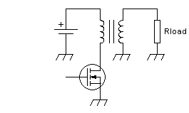
In fact this is the way many such amplifiers are built.
When the turns ratio required is close enough to 1:2 or 2:1, the
transformer's
size and cost can be shrunken quite effectively by using an
autotransformer:
Since the autotransformer provides no galvanic insulation, the coupling
capacitor again becomes necessary. But the small autotransformer has
better coupling and lower parasitics, and thus gives a better frequency
coverage.
This autotransformer is often made with a bifiliar winding, and then
it's often drawn in this way:
It's simply the same thing drawn differently. Some authors claim that
these bifiliar transformers are transmission line transformers, but
that's a matter of debate and definitions. And so it's time for the
next Blue Block:
Transformers:
Conventional, transmission line, real and fake ones
A conventional transformer consists of two or more windings that share
a single magnetic core. Any magnetic field caused by current flowing in
one winding will induce a voltage in all windings. This
allows a transformer to transfer energy from one winding to the others,
and by making windings with different turn numbers, it can also convert
one combination of voltage and current into a totally different one,
keeping the power constant except for some slight losses. It is a very
versatile device, that found many applications in electricity and
electronics even before Adam invented the vacuum tube. But it has
important drawbacks too, called "parasitics". And the big problem for
us, when building RF power amplifiers, is that in RF power applications
these parasitics are particularly nasty.
All real-world conventional transformers have less than perfect
coupling between their windings. This shows up in their behavior as if
there were additional inductors connected in series with their
windings, these little inductors having their own separate magnetic circuits,
being uncoupled to the main transformer. As the frequency gets higher,
this "leakage inductance" ends up making a transformer unusable. In
most RF power applications, leakage inductance is what determines the
upper frequency limit at which a conventional transformer can work well
enough. It is possible to reduce the leakage inductance by intimately
mingling all windings, for example by using twisted wires to wind all
windings together, but this increases another parasitic, which is
the capacitance between windings. There is no free lunch here,
only a chance to make the best compromise.
The allowable wire length of a winding is limited by the simple reason
that current only flows at a speed close to the speed of light. The
wire length has to be much smaller than the wavelength, for the
transformer to function normally. At HF this can already start to
become a problem, while at VHF it's a serious problem. And even in HF
amplifiers, transformers are often expected to carry non-sinusoidal
signals, which means that there are harmonics present that reach high
into the VHF range, and even into UHF. So, winding wire length can
become a critical factor even at HF.
The larger a conventional transformer is, the higher are these
parasitics. But in high power applications we need rather large
transformers, to handle the high voltages and currents, so this is bad
news, and ultimately limits the applicability of conventional
transformers in RF power amplifiers.
Transmission line transformers instead work on a completely different
principle: One or more transmission lines of a properly chosen
impedance, carrying RF energy from the input side to the output side,
and having something on them that makes the output side not "see" the
input side, except through the line proper. This "something" is usually
a magnetic core on which the
transmission line is wound, which makes the line act as a common-mode
choke: Any differential current on the two conductors can pass freely,
while all common-mode current is largely blocked by the inductance or
impedance of the line wound on the core.
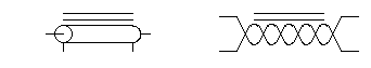
The transmission lines can be coaxial cable, parallel line, twisted
pairs, etc. Some people draw transmission line transformer sections as
coax conductors with a core, or twisted lines with a core, or even two
windings on a core. The core is sometimes drawn using the standard
schematic symbol, but some designers prefer to physically draw a toroid
around the line. There is much creativity in this area of electronics
art. I prefer to draw them either as twisted line or as coax line, with
a symbolized core, like this:
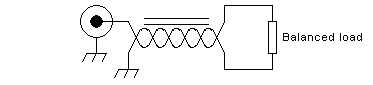
A single transmission line on a single core can be used as a balun: One
end of the line has one conductor grounded, the other conductor
connected to an unbalanced signal source. The other end of the line has
the same signal voltage between its conductors, at the same signal
current, but is no longer ground-referenced. It's a floating,
differential signal source. It can be used to drive a balanced load:
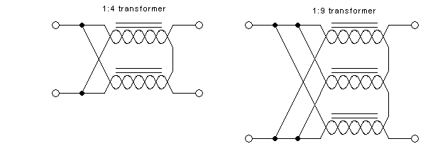
What's more fun is that two such transmission lines, each of them wound
on its own core, can be connected with their inputs in parallel and
their outputs in series, thus implementing a transformer with a 1:4
impedance ratio. This principle can be extended to three lines and
cores for a 1:9 transformer, and so on. These transformers can be
freely used with balanced or unbalanced circuits on each side, since
they all also provide balun functionality.
The beauty about these transmission line transformers is that they
almost don't have a practical upper frequency limit. Even when the
transmission lines are long relative to the wavelength, they are all
the same length, and so the output signals from all of them are in the
same phase, allowing series connection of the line outputs.
Whenever the transmission lines used to make such transformers have an
appreciable length, relative to the wavelength of the highest
frequency at which we want them to work, they need to have the
same impedance as the signals they are carrying. For example, if the
1:4 transformer shown above is to be used to match a 12.5Ω source to a
50Ω load, then each of the two transmission lines needs to have a 25Ω
impedance. The two line inputs in parallel will match to the 12.5Ω
source, and the two line outputs in series will match to the
50Ω
load. In many practical situations it will be necessary to construct
transmission lines of the proper, specific impedances. In other cases
it may be necessary to wind such transmission line transformer
elements with two or more coax cables and connect them in
parallel, to achieve a low impedance. For higher impedances it will be
necessary to use parallel transmission lines. And transformers for
extremely high or low impedances can be hard or impossible to
make.
In some
situations, when the maximum operating frequency is low enough so that
the line length is very short compared to the wavelength, one can save one transmission
line and its core, by connecting the line outputs in series with the
signal input:
This configuration gets many different names, among them "bootstrapped
transmission line transformer", "false transmission line transformer",
"non-equal delay transmission line transformer", among various
others. The point to keep in mind is that this kind of configuration
does have a strict upper frequency limit, given by the requirement that
the transmission lines be very short relative to
the wavelength. The balun effect is also lost.
This circuit could be redrawn in this way, for improved clarity:
And many people claim that this is nothing else than a combination of
two autotransformers,
which could also be drawn like this:
So, it is important to remember one very important point: When you see
a combination of transmission lines wound around cores, in which each
line's end is connected either
to the input side or
the output side, it's a true transmission line transformer that has
a very wide frequency range. Instead if you see lines that
have the two poles of the same
end connected to the input and
output circuit,
then it's not
a true transmission line transformer, but one of those
contraptions that suffer from the same wire length limitations as
conventional transformers do.
Single-transistor tuned amplifiers:
Instead of using a choke to feed the supply current into the amplifier,
and use transformers to adapt the load impedance, it's possible to do
both tasks using tuned circuits. The disadvantage of this approach is
obvious: The amplifier will only be usable inside a relatively narrow
frequency range. But in many cases this is acceptable and even
desirable, for example in single-band radios. And there are
various advantages in using tuned circuits: They typically don't need
ferrite cores, which eliminates some cost and weight, and also does
away with all the characteristic problems of ferrite materials, such as
losses, DC saturation and nonlinearities.
The narrow-banded nature of tuned circuits makes them suppress
harmonics, and this allows operating these amplifiers in classes other
than class A. Tuned linear amplifiers can be easily built using a
single transistor, with far better efficiency than class A broadband
amplifiers. And class C tuned amplifiers, while typically nonlinear,
can easily achieve practical efficiencies of roughly 80%.
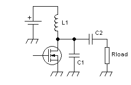
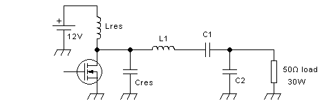
The basic single-transistor tuned amplifier's output section looks like
this:
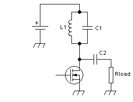
As you have immediately spotted, it's the same basic circuit as the
broadband one, except that the choke has been replaced by a parallel
tuned circuit. This tuned circuit is resonant at the operating
frequency, or more typically at the center of the desired operating
frequency range. It has a Q factor suitably selected to meet several
goals: Higher Q leads to smaller bandwidth, better harmonic
suppression, smaller inductor, larger capacitor, higher loss and more
critical tuning. So the Q is a compromise, but many designers tend to
use a loaded Q of roughly 3 in a typical situation. This means that at
the operating frequency both L1 and C1 have one third as
much reactance as the resistance value of the load.
The inductive reactance of a coil is
Xl = 2 π F L
and the
capacitive reactance of a capacitor is
Xc = 1 ÷
(2 π F C)
where of
course F is the frequency in hertz, L the inductance in henry, C the
capacitance in farad, Xl the inductive reactance in ohm, Xc
the
capacitive reactance in ohm, and π is roughly 3.1416.
It's very usual to connect C1 from the drain to ground rather than in
parallel to L1. It works exactly the same, because the top end
of L1 is grounded at RF through the battery, or in a
practical circuit through the bypass capacitors installed at that
location. The circuit then would look like this:
As you can see, C1 ends up directly in parallel with the
transistor's output side, which means that the transistor's output
capacitance, if significant, needs to be subtracted from the value you
use for C1. This is true just the same if C1 is placed in parallel to
L1, by the way.
The relationships between supply voltage, drain voltage, load
resistance and output power are exactly the same as in the broadband
amplifier. But tuned amplifiers are typically biased to a much
lower standby current, operating in class AB, or even to no standby
current at all, operating in class C. It's interesting to understand
what currents will flow in such a case: The resonant circuit
L1/C1,
if it has a high enough loaded Q, will always force a nearly sinusoidal
voltage at the drain, and at the same time can source or sink any
instantaneous current needed to achieve this. This is a very different
behavior from that of the choke in the broadband amplifier, which
delivers a constant current over the RF cycle, regardless of the drain
voltage waveform. We can also think of this in the frequency domain:
While a choke has a high impedance over the whole RF spectrum of
interest, a resonant circuit has a high impedance at the fundamental
frequency, but low impedance at its harmonics and all other out-of-band
frequencies .
Whenever
the transistor is driven on, it will draw a current from the load and
the resonant circuit, defined either by the instantaneous gate voltage
(while in active range) or by whatever current is available to be drawn
(when saturated). As the transistor draws current pulses, over the
course of several RF cycles the resonant circuit increases the sine
voltage
amplitude across it, until reaching equilibrium either with the total
average current drawn by the transistor and the current delivered to
the load, or until the transistor saturates and the RF voltage gets
clipped to the supply voltage. MOSFETs conduct in both
polarities when driven on, and this will limit the peak RF voltage to
roughly the supply voltage, because the drain can't go significantly
negative. BJTs instead do not conduct collector-to-emitter when
reverse-polarized. But the base-collector junction does turn on, and
this pulls the base voltage down in such a situation, also limiting the
collector voltage swing. The clamped RF voltage, applied to the load
resistance, defines the load current, and this in turn limits the
average current that the transistor can draw. Of course, as the
conduction
angle of a class C amplifier is reduced, the peak current in the
transistor increases, for a given output power.
If a perfect (fully linear) transistor is biased for class B operation,
the amplifier will be linear, despite the transistor amplifying only
one half of the RF waveform, and staying completely off during the
other half. If a real-world transistor is used, which has a somewhat
nonlinear transfer curve, acceptable linearity for most
purposes can be achieved by biasing the transistor into class AB, with
the amount of idling current optimized for lowest distortion.
The very
fact that RF power amplifiers can be linear even when the transistor is
completely off during half of the time, puzzles many newcomers
to RF,
and this raises the need for another of my Blue Blocks:
Linearitity at RF and
audio - two different worlds
Audio fans are used to just one kind of linearity: The
amplifier is
supposed to deliver an output signal that is an exact copy of the input
signal, except that it has been enlarged. Since audio equipment needs
to process a wide wide frequency range, such as 20Hz to 20kHz, a
1:1000 range, and many individual frequencies are usually present
simultaneously over
this wide range, forming a complex waveform which is often asymmetric,
there is really just one way to achieve the required
linearity: At every instant the amplifier has to produce an output
voltage that is exactly proportional to the input voltage, the
relationship being set by a fixed gain factor which stays constant over
the whole frequency range.
But in most kinds of RF work, we don't have such wideband signals. A
typical ham signal might have a center frequency of 14320kHz, but a
total bandwidth of just 3kHz. That's a bandwidth of just 0.02%, so
narrow that on a scope it looks like a single frequency. For this
reason the waveform of a ham radio signal will always
be extremely close to a perfect sine wave, and since we know the waveform,
there is no need to make the amplifier painstakingly reproduce it. We
can allow the amplifier to brutally distort the waveform, and then use
a
frequency-selective network to eliminate the harmonic frequency
components,
which fully restores the original sinewave shape. The amplifier only
needs to create an output signal whose power varies in exact proportion
to the drive power, and that has the same phase modulation, if any, as
the input signal. If the amplitude and phase are right, and the sine
waveform is reconstructed by frequency-selective networks, then the
amplifier will be just as linear for a narrow RF signal as an
amplifier that offers perfect waveform reproduction of any input signal.
So, remember: If an amplifier accurately reproduces both the amplitude
modulation and the phase modulation of the input signal, it's a linear
amplifier for all narrow signals at RF. Waveform linearity is
absolutely not required, but typically the sine waveform needs to be
reconstructed by filters, to avoid unacceptable harmonic distortion
causing interference on higher bands.
Audio guys can't do that, given their complex, wideband signals. On the
other hand audio guys get the advantage of transistors that are
thousands of times faster than their signals, and that have extremely
high gain at their frequencies, so they can easily build
waveform-linear amplifiers. We RF guys have a much harder time
doing so, because the available transistors are slow and have low gain
at
our frequencies, and even a few cm of circuit board trace cause a
phase delay that could be many degrees of our signal's period. So we do
whatever
is simplest and most cost-effective in achieving our goal, and very
often this is building
amplifers that have extremely poor waveform linearity but good-enough
amplitude and phase linearity, and then we clean up their output
waveform using
resonant circuits or lowpass filters.
Since in most situations we need to design the amplifier for
a load resistance which is different from the drain load
needed to
produce the desired output power at the available supply voltage, we
need a matching network.
The simplest possible tuned matching network
is the L circuit. It's called L because it looks like a
lying-down letter L, consisting of either a series coil and a
parallel capacitor, or the other way around. The first option has some
lowpass behavior, the second one is rather a highpass. Since usually we
need to suppress harmonics, the lowpass version is by far the most used
one. The parallel element is always placed at the side of the L network
where the higher impedance is.
The equations for calculating the values for a lowpass L matching
network are the following:
Xl = √ ( Rlow × Rhigh - Rlow² )
Xc = Rlow × Rhigh ÷ Xl
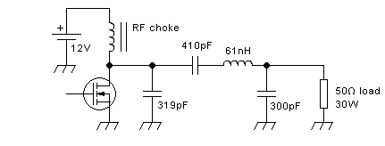
Let's calculate the values for a 12V powered amplifier that delivers
30W into a 50Ω load, like in the broadband example given above. There
we found that we needed a transformer with a 1:5 turns ratio, giving us
a 1:25 impedance ratio, thus transforming the 50Ω load resistance down
to a 2Ω drain load. Let's do the same with a tuned L matching network:
Xl = √ ( 2 × 50 - 2² ) = 9.80
Xc = 2 × 50 ÷ 9.80 = 10.2
So we need a coil having 9.80Ω inductive reactance at the design
frequency, and a capacitor having 10.2Ω capacitive reactance. If we
want to build this amplifer for the amateur 6 meter band, we design it
for the center frequency, 52MHz. Applying the reactance equations given
higher up in this page, we end up with a 30nH coil and a 300pF
capacitor. Note that a 30nH coil might need just two turns of
wire, with a small diameter! This is why in amplifiers that work at
much higher frequencies than this one, such coils are no longer
practical, and circuit board traces (microstriplines) are used instead.
And the 300pF capacitor looks easy at first sight, but it's important
to make sure that it has negligible stray inductance. A capacitor with
wire terminals isn't a good idea here. A parallel combination of two or
more
SMD capacitors works well.
Such a circuit almost always will need to be tuned after building. It
is possible to use trimmer capacitors, while such small coils are most
easily trimmed by deforming them, mostly changing the separation of
their turns.
While we are at it, let's quickly calculate the resonant circuit at the
drain: For a loaded Q factor of 3, and given the drain load resistance
of 2Ω, we need reactances of just 0.67Ω! At 52MHz this translates into
an inductance of barely 2nH, and a capacitance of 4.57nF. The drain
"inductor" would be just 2 or 3mm of straight wire, while the capacitor
would need to be made from several very small SMD parts in parallel to
achieve low enough stray inductance.
So these are quite impractical values. I chose this example to
illustrate the sort of difficulties often encountered in RF power
amplifier design: Very low impedances, requiring impossible components.
An amplifier like this, delivering 30W from 12V with a pretty clean
sine wave at the drain and a simple L matching network, can often be
made in the lower HF range, but hardly at higher HF, let alone VHF.
That's one reason why VHF amplifiers typically either work in some
other class, such as class E, or else have low efficiency.
We can start making compromises, to get our 52MHz 30W amplifier to
operate well enough. The most obvious one is lowering the Q of the
resonant circuit, to end up with workable components. The problem is
that as we reduce the Q, the waveform at the drain distorts, and we can
no longer obtain the power we expect without getting high drain voltage
peaks. If we retune the matching network
to deliver the desired power while using a very low Q drain tank, the
result is sky-high drain voltage peaks, which in the best case reduce
the efficiency of the amplifier, and in the worst case destroy the
transistor.
Reducing the tank Q to unity, resulting in a 6nH coil and a 1.5nF
capacitor, we still get the desired power, at a peak drain voltage of
only 27V, instead of the 22V we got with a Q of 3. This is more
workable. Reducing it further, to 0.5, using a 12nH coil and a total
capacitance of 750pF, which includes the transistor's output
capacitance, the drain voltage waveform gets very ugly, but the circuit
still works well enough, and our component values start becoming
practical. Below that level the drain voltage waveform definitely
becomes too peaky, deformed, and the output power falls off
dramatically.
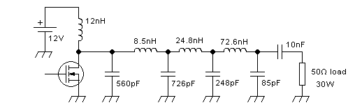
So, our 12V, 30W output section for the 50-54MHz band might end up
looking like this:
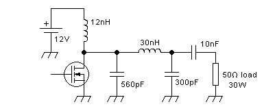
The 560pF is tentative, subject to confirmation of the output
capacitance of the transistor chosen. The 10nF capacitor serves just a
DC blocking function. Its reactance at the operating frequency is low
enough to have no significant effect. I placed it at the output side of
the L network, because there the RF current is much lower than at its
input side, and the DC voltage across the capacitor stays the same.
When building such an amplifier it's absolutely critical to minimize
stray inductances. The 560pF capacitor needs to be soldered directly to
the transistor's body, not one centimeter away. It needs to be a chip
capacitor, because any wire terminals at all will contribute too much
stray inductance. It's best to split it up into two capacitors of half
the value, and solder them to the transistor on both sides of the drain
terminal. Any deviation from this will make the amplifier behave less
like the calculation indicates. And even if you follow these
recommendations, you need to keep in mind that this design method is
very simplistic, for example by not considering the inductance of the
drain connection inside the transistor. One can usually get away with
such simplifications at HF, but at 52MHz it's risky, and on even higher
bands it definitely no longer works well enough. At VHF and higher one
needs to design the matching network for the load impedance the
transistor needs at its drain terminal, and not the one it needs
inside,
at its actual drain on the silicon chip. This load impedance needs to
be looked up in the data sheet, which usually gives it for a single or
a few operating frequencies and power levels. It often needs to be
interpolated, if your application is not a completely standard one for
the chosen transistor.
The L matching network is by no means the only choice for such a simple
amplifier operating in class AB or class C. In fact, very often there
are better choices. That's because the L network doesn't allow you to
choose the loaded Q of the network. The Q of an L network is
Q = √ (Rhigh ÷ Rlow -1)
So in this example the loaded Q is 4.9. One of the implications of this
is that the network has a -3dB bandwidth of roughly one fifth the
center frequency. The usable bandwith is even less, because 3dB power
drop at the band edges is not acceptable in a power amplifier. But
since the amateur 6 meter band has a width of one thirteenth
of
the center frequency, the bandwidth of this network with a Q of 4.9
would be sufficient. But there may be other applications in which more
bandwidth is needed, making a lower Q desirable. Or there might be a
more stringent requirement for harmonic suppression, making a
higher Q desirable.
Also it's important to consider the stress placed on the components. A
loaded Q of 4.9 also means that the network is storing 4.9 times as
much reactive power, as the output power is. So, this little network is
storing nearly 150W of reactive power! Even if you make the tiny 30nH
coil from really thick wire, it might still have enough RF resistance
(which is far higher than its DC resistance, due to skin effect) to
heat up so much that it unsolders itself from the circuit! You might
need really
thick wire
for it, or perhaps use silver-plated copper sheet. The silver
plating helps just a tiny bit, but using sheet instead of round wire
helps a lot.
Likewise, the 300pF capacitor is under high stress. It works at the
full output voltage of 39V RMS, but also at nearly the full input
current to the network, specifically at 3.8A RMS. You need a capacitor
rated for at least this much ripple current, and that's typically a
"transmission type" capacitor, such as a porcelain chip capacitor, or
at least a very high quality NP0/C0G chip type. If you use a
trimmer, it also needs to be able to handle that much current. A small
cheap flimsy little trimmer won't do it, but a big, hefty, sturdy one
will have way too much stray inductance. You need a small, high quality
trimmer made for transmitter applications. Which is why experienced
designers try to avoid using trimmers in such places.
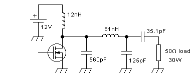
If you would like to increase the loaded Q, for better harmonic
suppression, there are several networks that allow doing it. The most
common of these is the LCC network, meaning one coil and two
capacitors. It looks exactly like the circuit we already have, and the
only change is that instead of using a large value DC blocking
capacitor (10nF in my example), we reduce the size of this capacitor to
make it an important part of the matching network. To design this
network, you pick the value of loaded Q you want, which must be higher
than the Q the L network would have, and then you use these equations:
XL = Q × Rlow
XC1 = Rlow ( 1 + Q² ) ÷ ( Q - √ ( Rlow ( 1 + Q² ) ÷ Rhigh -1)
XC2 = Rhigh √ ( Rlow ( 1 + Q² ) ÷ Rhigh - 1 )
Applying these equations to our example of the 12V powered 30W
amplifier for 52MHz, and setting the Q at 10 (which is higher than
usual, but OK for this example), the inductor turns out to need a
reactance of 20Ω, and thus an inductance of 61nH. The first capacitor
needs to have 24.46Ω of reactance, which results in 125pF at this
frequency. And the second capacitor, the one that was just a coupling
capacitor when using an L network, now needs to have a reactance of
87.2Ω, and thus a capacitance of 35.1pF.
Hint: When using equations like the ones above, be very careful about
using the correct precedence of operations! While that's just sixth
grade maths or so, it's still easy to make a mistake.
Our amplifier's output section, with the loaded Q changed to 10, ends
up
looking like this:
Another way to raise the Q is to place a series resonant circuit in
series with the inductor of the L network. The two inductances that end
up in series can of course be melted into a single inductor of the
total inductance value. The circuit then looks like this:
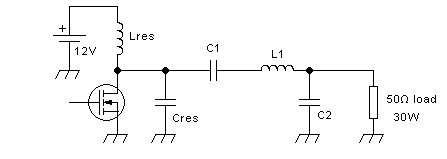
or like this, whichever you like best:
The design equations for this network are the following:
XC1 = Q × Rlow
XL = √ ( Rlow × Rhigh - Rlow²) + XC1
XC2 = Rlow × Rhigh ÷ (XL - XC1)
So, for our 12V 30W 52MHz amplifier, designed with a Q of
10, XC1 is 20Ω, XL is 29.8Ω, and XC2 is 10.2Ω. This equates to
153pF, 91.2nH, and 300pF. Lres and Cres of course are resonant with
each other at the operating frequency, with a Q high enough to maintain
a reasonable sine wave, and low enough to not limit the bandwidth too
much and to have practical values, and Cres includes the transistor's
output capacitance.
The -3dB bandwidth of these networks with Q = 10 will be only 5.2MHz,
so they are really a bit
too narrow to cover the entire 6 meter band with near-flat response. Q
factors as high as 10
are rarely used in solid state amplifiers. They were more typical in
tube amplifiers, where a high Q was necessary to allow the high
impedance ratios needed there, and to absorb the sky-high output
capacitance of tubes. But tube amp users had to pay for that
by tuning up their transmitters to the specific frequency they wanted
to transmit on.
In solid state practice it's more common to try achieving larger bandwidth,
be it to cover a wide band without retuning, such as 88 to 108MHz for
a frequency-agile FM broadcast transmitter, or be it to
mass-manufacture a design
without having to individually tune up each unit. More broadbanded
matching networks are less critical in terms of component tolerances
and accurate placement on the board.
There really aren't too many options when it comes to making low Q
tuned matching networks. The best approach at HF and low VHF is
probably cascading several L networks. In this case each L network has
a much lower Q than a single L network, and the combination of all of
them has a higher Q than the individual L networks composing it, but
lower than a
single L network that does the entire transformation.
Let's try modifying the amplifier to use this approach, with three L
networks cascaded. Each of them will transform over the same resistance
ratio. Since the total ratio is 1:25, each L network needs to have a
ratio of 1: 2.924, because the cubic root of 25 is 2.924. And each L
network will then have a Q of 1.39. So, our first L network
matches 2Ω to 5.85Ω, the second one matches 5.85Ω to 17.1Ω, and the
third one matches 17.1Ω to 50Ω. Applying the equations for the L
network to each stage, the circuit ends up like this:
The -3dB bandwidth of this circuit is nearly 3 times wider than for the
simple L network. And the -1dB bandwidth, which is a more useful
characteristic for power amplifiers, improves more than threefold, from
around 10MHz to 33MHz.
The inductances in such a circuit get so small at VHF that they are
usually implemented as a single microstripline on the printed circuit
board, with the capacitors soldered to that strip at
strategically selected locations, to implement the proper
inductance between each capacitor and the next one. Sometimes the width
of the microstripline is adjusted for the different inductance values:
It starts very broad at the transistor, and then narrows down after
each capacitor. At HF instead
discrete coils can be used, but it's not very common to use this sort
of
wideband tuned amplifier at HF, because single HF bands are usually
narrow enough to use a simpler matching section, while to cover several
bands one needs a true broadband amplifier anyway. Instead a very
common application for such a network is a commercial VHF radio
covering 136 to 174MHz.
The tuned matching networks that I have described here just barely
scratch the surface, but tend to suffice for typical practical
amplifiers. There are many other possible configurations, including Pi
and T circuits. But not all of those lead to practical component
values. And there are many web pages devoted exclusively to impedance
matching, and some of them include online impedance matching
calculators, so if you are particularly interested in tuned impedance
matching, you should search and read some of those pages.
One more comment is due at this point: The data sheets of RF power
transistors give the required load impedances,
not just load
resistances, because a typical transistor does need some reactance in
the load at most frequencies, to compensate for its output
capacitance and for its lead and bonding wire inductance. It's a simple
matter to take the series-expressed complex impedance value from the
datasheet, design your matching network for the resistive part of that
impedance, and then add the required reactance in series with the input
of your network, by either reducing or increasing the first inductor's
value by the appropriate amount, depending on wether the transistor
needs a capacitive or inductive component in the load impedance.
People who are too lazy to do these maths will simply design an
approximate matching network, and make two of its elements adjustable.
Then they will tune up their amplifiers for best power output and
efficiency, by adjusting trimmers or deforming coils. In the case of
amplifiers for HF, it's often practical to use coil formers
with
adjustable slugs in them.
All of these tuned output sections are suitable for use with all
traditional classes of operation: A, AB, B and C. Instead the
single-transistor broadband configuration is really good for
class
A only.
Class E
No, don't worry, I do know the alphabet, and I haven't
forgotten
class D. But class D amplifiers most commonly use two transistors
rather than one, and we aren't there yet, so I will treat them later.
Class E amplifiers instead are commonly built around a single
transistor, and look extremely similar to the tuned amplifiers we were
just busy with, and so it makes a lot of sense to treat them now and
here.
Class E amplifiers were developed to improve the efficiency beyond that
of a class C amplifier. They always operate with the transistor driven
into full saturation and full cut-off, either by using a squarewave
drive signal, or by strongly overdriving them with a sinewave. This is
the first step in achieving high efficiency, because a fully saturated
transistor can only cause a small conduction loss, and a transistor
that is off cannot cause any significant loss at all. Class D
amplifiers
do the same. But there is a big problem with class D: Transistors
simply cannot switch fast enough to keep the transition time
insignificantly small, at radio frequencies. Class E tries to eliminate
most of the switching loss by using an output network that shapes both
the drain voltage waveform and the drain current waveform, trying to
achieve a drain voltage as close to zero as possible while the
transistor is switching on, and trying to keep the drain current as
close to zero as possible while the transistor is switching off.
The circuit required to do this is almost the same as in the amplifiers
we were just looking at. The main difference is that since we will be
controlling the drain voltage waveform with our matching network, we
don't want any other resonant circuit at the drain. So we replace the
resonant inductor that feeds the supply current to the drain by an RF
choke, which forces a constant supply current over the RF cycle,
allowing
strange and even abrupt drain voltage waveforms.
Did I say "RF choke"? Yes. And while discussing class A
broadband amplifiers, I talked just about chokes. Time for another Blue
Block:
Chokes and RF chokes:
A choke is an inductor of such a high inductance value that it blocks
all alternating current that would want to flow, as much as possible.
That is, a choke carries essentially a pure DC at all times, as far as
imperfections and design compromises allow.
But a choke in a real-world circuit really doesn't need to fully block
all frequencies from a femtohertz to a petahertz and beyond. Nor could
we make such a choke. In practice, we just need the choke to block the
frequencies that we want blocked. Sometimes this could be all
frequencies present in a circuit, but at other times we might want a
choke to block a certain (usually broad) range of frequencies, but pass
another (very different) range of frequencies.
In RF amplifier work we are usually dealing with two such broad
frequency ranges. One of them is radio frequencies, usually spanning
from the lowest frequency of operation, to the highest important
harmonic of the highest frequency of operation. For an HF amplifier
operating from 1.8 to 54MHz, the RF range to block might span 1.8 to
500MHz or so.
The other frequency range we must not forget is the envelope
frequencies. That is, the frequencies contained in any amplitude
modulation of our signals. In an AM signal, this range is directly the
audio frequency range our transmitter passes. In SSB the range is
wider, theoretically infinite, but from a practical point of view the
important components extend to about 10 times the highest audio
frequency our transmitter passes. Even a Morse code signal contains a
significant modulation bandwidth, which must be cleanly processed by
the amplifier to avoid deformed keying and the resulting key clicks.
In RF power amplifiers usually all chokes need to block the RF range.
We rarely if ever use chokes that deliberately have to block the
modulation frequencies, since such chokes would be big, heavy,
expensive, and inefficient. But for chokes in some positions
it's irrelevant whether or not they block the modulation frequencies,
while for others it's essential that they don't block them! In my
opinion it's important to be aware, during amplifier design, whether a
choke must freely pass modulation frequencies, or whether it doesn't
matter how well it passes them. If you use a choke that noticeably
affects the higher modulation frequencies, in a location where the
choke needs to pass them, the choke will distort the transmitted
signal! Many people have run into distortion trouble they don't
understand, due to using a choke that has too much inductance and thus
affects the higher modulation frequencies.
For this reason, throughout this article I'm making an intentional
difference between chokes and RF chokes. When I use the term "choke", I
mean an inductor that reasonably blocks all RF current, without you nor
me needing to care whether or not it also has a noticeable effect on
modulation frequencies. Instead when I write "RF choke" I mean an
inductor that has enough inductance to block RF currents well enough,
while having low enough inductance to pass all modulation frequencies
without any noticeable impact on them.
There is another point about chokes that I would like to briefly
mention: Many chokes are far from having a pure inductance.
Instead they have an impedance, that is, inductance in series with
resistance, and both the inductance and the resistance change with
frequency. Some chokes are almost purely resistive at the higher
frequencies. This behavior is fine, as long as the resistance is high
enough to keep the losses acceptable. After all resistance dissipates
power, while inductance does not.
It is often even desirable for a choke to be more resistive than
inductive, because this reduces the risk for resonances, reduces
phase shifts, and thus contributes to amplifier stability. But of
course any choke needs to have a low enough resistance to DC, and RF
chokes also need to have a low resistance to all
modulation frequencies too.
The amount of impedance a choke needs to have, of course depends on the
circuit impedances. A typical rule of thumb is making sure that the
choke has at least 10 times as much impedance as the circuit it's
connected to, at all frequencies in the range it has to block, but
specific applications might need even better choking, while others can
work well with a significantly lower choking impedance. Typically if
the choke's impedance is mainly resistive it needs to be higher than if
it's mostly inductive, to keep the losses at an acceptable
level. A factor of 100 is more common than 10, for a mostly
resistive choke.
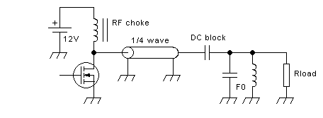
A typical, practical, class E amplifier's output section will look like
this:
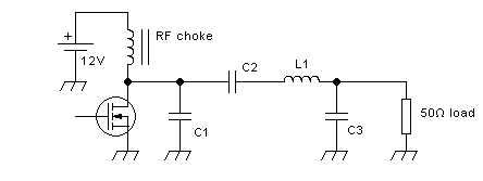
No big surprises there, huh? You might ask what's new at all!
The
only difference that can be seen, between this class E amplifier and a
typical tuned amplifier that can be run in class A, AB, B or C, is the
use of an RF choke instead of a small tuned inductor. Even
this
difference isn't absolute, because class E amplifiers can be designed
to work with a small tuned inductor there too, although they work the
cleanest way when an RF choke is used, that is, the current supplied to
the circuit is forced to be a pretty smooth DC over the entire RF
cycle.
The main difference is in the way to calculate the component values.
The design equations for a class E amplifier are pretty complex, and
that's why I won't copy them here, and rather suggest that you use any
of the several online calculators and design programs that exist for
class E amplifiers. Most of these calculators, and also the equations
given on websites, are applicable to a textbook circuit like this:
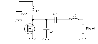
You can punch the values you want for voltage, frequency, and power
into one of those online calculators,
including the value you pick for L1, and get values for C1, C2, L2 and
Rload. If you pick a relatively large inductance for L1 the circuit
will work better. A very low value for L1 might make you end up with
the need for negative capacitances or negative inductances somewhere...
And yes, Rload is calculated too, and would be 2Ω or very close to it,
if you try our exercise of a 12V 30W 52MHz amplifier. If you need a
different load, you have to add a matching section to that circuit. The
simplest one is the L, of course, so you calculate an L circuit to
match 2Ω to 50Ω and add it, and since that makes you end up with two
inductors in series, you can merge the two into a single inductor that
has the total inductance value.
Doing this for our 12V 30W 52MHz example, choosing a Q of 5
for the
basic class E network, and using an RF choke that has high impedance at
52MHz, makes us end up with these values:
Don't forget that you need to drive this transistor with a squarewave,
or with a pretty strong sinewave. You will be rewarded with a high
efficiency, that could be as high as 90% if you use a good transistor,
but you also have to be aware that the normal voltage peaks at the
drain will be at least 3 times the supply voltage, and during transient
conditions could be even higher. So you need a transistor with a higher
voltage rating in this circuit, than if you use a very similar looking
circuit operating in class A, AB, B or C with a sinewave
voltage
at the drain that doesn't even reach twice the supply voltage.
Many designers have tried to make a class C amplifier, for example for
an FM transmitter, and then have empirically tuned and tweaked the
matching network, while putting nice strong drive to the transistor,
until reaching efficiencies above 80%. In fact they ended up with class
E amplifiers, without even knowing it!
Since class E amplifiers operate in saturation, any amplitude
modulation of them, even on/off keying for Morse transmission, should
be done by modulating the supply voltage with a suitable waveform,
while keeping the drive signal going.
Class F
In order to get higher power from a given transistor, without exceeding
its drain voltage rating, someone came up with the idea to shape the
drain voltage waveform into a square wave, by designing an output
network that offers a short circuit to all even harmonics, but an open
circuit to all odd harmonics. This was done by placing a parallel
resonant circuit in parallel with the load, which offers a short for
all harmonics, and then connect it to the transistor via a
quarter-wave-long transmission line,
like this:
A quarter-wave-long transmission line has the interesting
property
that on all even harmonics it reflects the same load impedance
it
sees at its end, while on all odd harmonics, and the fundamental, it
transforms the
impedance it sees to its image value as seen from the line impedance.
So, if we have a load resistance
of 50Ω, a resonant circuit tuned to the working frequency, and a
quarter-wave-long 10Ω transmission line, then at the working frequency
the
drain will see a 2Ω load. At all even harmonics it will see the short
circuit offered by the resonant circuit. And at all odd harmonics it
will see the short circuit of the resonant circuit transformed by the
line into an infinite impedance, that is, an open circuit. So the drain
voltage will become a square wave, and the drain current too.
In
theory it all works very
nicely, and the efficiency should be very high, along with a
higher power output from a given transistor, if the proper
supply voltage is chosen. In practice however it's hard to get a
transmission line at UHF to perform just right. It would need to be
very thin, and then it can't handle high power. On HF instead such a
line would be too long to be
practical. And anyway, RF transistors don't like square wave voltages
on their drains, because that causes large losses due to the need of
charging and discharging the transistor's output capacitance at a very
high rate, and due to internal parasitic BJTs in MOSFETs turning on at
these very fast drain voltage transitions. So I don't see class F
amplifiers as being very useful in
the context of this article.
To make a class F amplifier of a sensible size for HF, instead of the
transmission line one needs to use several parallel-tuned circuits
(traps),
each tuned to one odd harmonic, installed in series in place
of
the transmission line, and then one needs to add an L network for the
impedance transformation. This tends to become too complex to be
practical, specially considering that the network will only
cover a single band, and the losses in the several tuned
circuits
tend to eat up any
advantages the circuit might otherwise have. So it's not common to see
class F amplifiers used for HF.
Broadband push-pull amplifiers:
Most HF amplifiers for radio purposes are broadband ones, not because
any broadband signals are to be transmitted, but because operation on
several bands is required. And given that single-transistor broadband
amplifiers need to run in class A to avoid massive harmonic output, and
class A is very inefficient, most broadband linear amplifiers for power
levels
above a few watt are usually push-pull designs, which provide better
efficiency by running in class AB or class D, or a
hybrid between those two.
The general form of a push-pull amplifier's output section is like this:
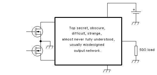
If you try to look up that output network in books about RF power
amplifier design, you will hardly ever find anything useful, either
because the book doesn't treat HF, or because the author has no faint
idea about the matter. If a book actually describes such a network, the
description is usually copied from an older book or magazine article,
and the book author copied it with all of the original faults and
misunderstandings. If you look into transistor datasheets and
application notes, you will find very few broadband push pull circuits,
because the application engineers at those companies don't understand
them either, get poor results when trying to build any, and the company
then prefers to publish some narrow-band design that works better and
thus puts their transistors in a better light.
So, let's tackle this matter piece by piece. The method is: Divide and
conquer. A very old and well-proven approach.
A push-pull output network needs to perform several functions. Some of
them are the same as those a network for a single-transistor amplifier
needs to perform:
- Inject the power supply to the transistors.
- Transform the load resistance to whatever value is needed between the
drains, for the available supply voltage and the required output power.
- Block the DC from reaching the load.
In addition, a push-pull output network has some additional tasks:
- Act as balun, to transform the single-ended load into a balanced load
between the drains.
- Tightly couple the drains together, in phase inversion. This function
is required for class AB and voltage-switching class D operation. In
class A it's not required, but doesn't hurt if present. For
current-switching class-D operation it must be absent.
- Restore a sinewave signal, through bandpass or lowpass filtering.
This is required in class D, but optional in class A and AB, depending
on whether the amplifier can provide the required harmonic suppression
just by operating very linearly. Most often it cannot...
- Properly handle or suppress common-mode signals. This may or may not
be necessary, depending on things like the type of feedback employed,
if any, the drive method, and the linearity of the transistors. I will
treat this point when getting to driving and feedback circuits.
A very simple and convenient way to implement all of these tasks,
except filtering, is to employ a conventional transformer having a
center-tapped primary:
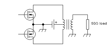
Since this circuit provides drain-to-drain coupling, but no filtering,
it's suitable for class A and class AB. If a filter is added, it can be
used for voltage-switching class D too. It could then also be
used
for class C, but that's rarely done. And class B is theoretically also
possible, but as explained way above, real-world circuits can never
truly work in class B.
The big problem with this nice and simple circuit is that its practical
implementation gets ever harder as the frequency gets higher, the
bandwidth gets larger, the power gets higher, and the supply voltage
gets lower. This is caused by the shortcomings of real-world
transformers, which never have perfect coupling. As the
frequency gets higher, the transformer needs to get smaller. But
smaller transformers might not offer enough inductance for operation on
low frequencies, might not handle the RF voltages without
excessive core heating, or might not allow using thick enough wire for
the currents that flow. At a given power, a higher supply voltage makes
leakage inductance less critical by a square factor, but the core needs
to be much larger too, or more turns need to be used, both of
which increases the leakage inductance and also the parasitic
capacitances.
If we had really good magnetic core materials, life would be
much
easier. But with the materials available today, it's hard enough to
make such a transformer that works well from 1.8 to 30MHz in a 12V 10W
amplifier, and I wouldn't know how to reasonably build such a
transformer for a 1.8-54MHz, 12V 100W amplifier. Let alone a 1.8-54MHz,
50V, 1.5kW one! Many 100W output stages use a conventional
transformer that has a two-hole core and a single-turn primary, but
this is not
the correct type of transformer for this circuit, because it
offers no coupling whatsoever between the halves of the primary. I will
get to that transformer, and its legitimate uses, just a little further
down this page.
One way to make the situation more manageable is to split up the
functions of the output network between two magnetic devices. One of
them is a thing sometimes called a "bifiliar choke", also called
"balanced feed transformer", and several other names, which injects the
power supply and couples
the drains. The other device is a conventional transformer that
performs the load resistance matching, isolation and balun
functions. The circuit looks like this:
Some people prefer to draw the feed transformer in some other way that
suggests its bifiliar construction, such as this:
But I feel that this looks like scratching my left ear with my right
hand, so I prefer the other drawing style, which also suggests very
well that this feed transformer performs some of the same functions as
a center-tapped primary winding.
Splitting up the functions between two transformers makes the task
easier, but still not really easy. In amplifier configurations
requiring drain-drain coupling, it's still hard enough to make a
bifiliar feed transformer that couples well from 1.8 to 30MHz, and very
hard if you want to get to 54MHz, as soon as the power level of the
amplifier is higher than about 10W at 12V, and 100W or so at 50V. It's
common to see ferrite toroids wound with 5 to 10 bifiliar turns, but
these suffer from so much leakage inductance that they don't properly
couple the drains in the higher part of the HF range.
By the way, a twin-hole core with a single-turn primary is perfectly
fine as the impedance-transforming, balancing, and DC-isolating device,
when combined with an effective bifiliar feed transformer - within its
frequency limitations, of course.
Instead of a conventional transformer it's possible to use
transmission-line transformers to do the load resistance matching and
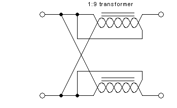
the balun action. An output section using a TLT with a 1:9 impedance
ratio
might look like this:
This circuit places a load resistance of 5.56Ω between the drains, and
also performs balun action. The true transmission line transformer has
a very wide frequency response, so one can pretty much stop worrying
about its
upper frequency limit. Each of the three transmission lines needs to
have a 16.7Ω impedance. The three lines in parallel give 5.56Ω at the
input, and the three lines in series give 50Ω at the output. If lines
of a wrong impedance are used, the transformer will still work at low
frequencies, but will become increasingly bad as the frequency rises,
because the lines will start doing some unwanted impedance
transformation on their own.
The uppermost line works at the highest end-to-end common-mode voltage,
so it also places the largest stress on its core. It should either have
the largest core, or the most turns. The lowermost line has the lowest
choking requirements, so it can use the fewest turns or the smallest
core. Since the lines should all have the same length, to maintain high
frequency performance, the best economical compromise is to use the
same length of line for each of the three, but use different number or
sizes of cores in each.
Since a TLT doesn't provide DC blocking, suitable blocking capacitors
have been added. I put them on the output side, where the
current is lower.
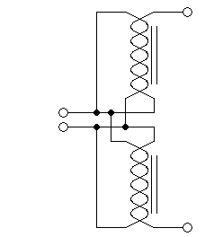
Sometimes a different configuration is used to achieve the same
purpose. The 1:9 transformer is implemented in a bootstrapped
configuration, saving one transmission line and its core. But then the
transformer doesn't provide balun action (common-mode current
blocking), and needs a separate balun (common-mode choke) added! The
circuit looks like this:
The two lines of the impedance-matching transformer now work at the
same end-to-end voltage, and thus are made identical. The balun works
at a higher end-to-end voltage and thus needs a larger core or
more turns.
Note that "larger core" in this context means a larger ferrite
cross-sectional area.
One could ask what point there is in replacing a true transmission line
transformer using three lines and three cores, by a bootstrapped
version that needs the same number of lines and cores but has a
definite and rather low upper frequency limit. The explanation is that
the latter version needs only 7/9 as much total ferrite cross section ×
turns product, as the former one! So, when every penny
counts, the latter version is cheaper, and might get the job done, if
the required top frequency isn't too high. But often it's impractical
to take advantage of this, and designers choose the simpler
solution of using only one type of core. Also the former
version has the flatter frequency response.
Now that we have a good solution for a very wideband load matching
system, it's time to look once more at the remaining trouble spot: The
coupling between the drains. Since it's too difficult in practice to
make split-primary transformers that produce the required excellent
drain-to-drain coupling, and in most cases with mid and high power
amplifiers operating to 54MHz it's also very hard or impossible to make
a bifiliar feed transformer that does this job, we are often forced by
practical reasons to consider amplifier circuits that don't need any
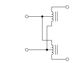
drain-to-drain coupling at all. For example, consider this output
section:
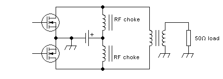
The power supply is now injected through two completely separate RF
chokes. They have absolutely no coupling between them, as shown
schematically by drawing two separate magnetic cores. Each of these RF
chokes will force a constant current over the entire RF cycle. The
current can change at modulation rates, though. Each drain can now have
its own voltage excursions, unbound and unlimited by the other drain.
This is much like having two single-ended broadband amplifiers, with
the load connected between their drains, rather than from one drain to
ground.
I drew this circuit with a conventional transformer at the output, for
simplicity, but the following discussion applies regardless of
whether conventional or transmission-line transformers are used for
load matching. In either case the load appears differentially between
the drains.
Such a configuration works well in class A, and in current-switching
class D. It cannot work correctly in class AB, class B, class C, and
voltage-switching class D. This is because those classes require the
total supply current to vary over the RF cycle, which cannot happen
when there are uncoupled and un-bypassed RF chokes in series
with
it. Instead class A and current-switching class D amplifiers work at a
constant
supply current over the RF cycle. Actually class A works with constant
supply current at all times, so it could even use wideband chokes
instead of RF chokes, if that was practical.
At this point it's important to understand the voltage and current
waveforms happening in a push-pull amplifier, in
each operating
class. For this purpose let's consider two output circuits that have
the load connected directly between the drains, so it's easiest to
imagine and analyze what's happening. Having a transformer-coupled load
behaves the same, but needs to consider the transformation
ratio
in all calculations.
One of these circuits has drain coupling, the other does not:
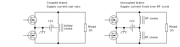
When operating in class A, using perfectly linear
transistors,
each of the transistor will conduct a DC (identical for both), plus the
full-wave RF current (in opposite phases). In this example, let's
assume that we set the DC at 8A per transistor. So, at the
zero
crossing, each transistor conducts 8A. The bifiliar choke, or feed
transformer, conducts 8A in each winding, and since they are in opposed
directions, there is no flux in its core. Both drains are at 12V, and
the load sees no voltage and no current.
At the peak of the signal, when the amplifier is driven
pretty
hard but not into saturation, one transistor is being driven to conduct
15A, the other instead is only driven to conduct 1A. Remember that
transistors basically behave as controlled current sources. The
bifiliar choke cannot suddenly conduct 15A in one winding and 1A in the
other, because that would make the net current in it rise from zero to
14A in a quarter of one RF cycle. So, for every ampere the current
increases in one winding, it also has to increase the same amount in
the other! The bifiliar choke forces this behavior. Also, due to the
coupling between the windings in opposed phase, and the fact that the
midpoint is held at constant voltage by the power supply, and by bypass
capacitors in a real circuit, whenever the voltage at one end rises,
the voltage at the other end must drop by the same amount. So this
bifiliar choke or feed transformer forces the two drain voltages to
maintain symmetry around the supply voltage.
The final result is that the current difference will have to flow
through the load resistance, since this is the only available path. The
bifiliar choke still conducts 8A per side, and on
the side where the transistor is driven softer and conducts only 1A,
the excess 7A flow into the resistor. At the other end of the resistor
these 7A come out and add to the 8A coming from the bifiliar choke, and
the
transistor on that side conducts the resulting 15A. The 7A in the 3Ω
load resistance cause 21V drop, and the bifiliar choke distributes this
drop
evenly around the 12V. So, the transistor conducting 15A sees its drain
voltage drop to 1.5V, while the other transistor sees its drain voltage
rise to 22.5V.
Of course during the opposite half cycle the transistors switch roles.
1.5V is probably as close to saturation as one can get without
excessive distortion, so this represents the maximum undistorted power
output for this amplifier. 21V peak equals 14.85V RMS, and
with the 3Ω
load chosen in this example, the power output is 73.5W. The supply
current stays constant at 16A all the time, so the input power is 192W,
and the efficiency is 38%, typical for a good class A amplifier.
Now consider the same class A operation with the circuit that does not
couple the drains. Since the supply current is constant in class A,
this circuit happens to work exactly the same! There will be the same
currents and voltages as with the drain-coupled circuit, although the
two separate chokes will each run with a considerable flux density in
their cores, because they conduct a big DC. But there is another
difference too: In this circuit there is nothing forcing voltage
symmetry around the supply voltage. If there is symmetry, it's caused
purely by the transistors being identical, the drive being perfectly
symmetric, and everything else also being symmetric. Any asymmetry
caused by real-world tolerances will manifest itself in different,
asymmetric voltage waveforms at the two drains, while the circuit with
a bifiliar choke will largely suppress them.
Now let's consider the nonlinearity of real transistors. Specially when
using MOSFETs, the gain is much lower at low currents than at high
ones. So, if the transistors are driven
symmetrically, they will not
conduct
symmetrically. When one is driven to 15A , the other one might
still be conducting 3A instead of the 1A it should. So the two of them
will conduct a total of 18A instead of the desired 16A. But at the zero
crossings each will conduct 8A, for a total of 16A. So the total supply
current will want to fluctuate between 16A and 18A, at twice the
operating frequency. And this opens a whole new world of complications
and trouble!
It's not really terrible when we are using a circuit with good
drain-to-drain coupling. In that case simply the amplifier will consume
a supply current with this small 2A ripple on it. The drain voltages
will stay symmetric around the supply voltage, because the bifiliar
choke forces it. At the signal peak, one transistor conducts 15A, the
other 3A, the bifiliar choke conducts 9A in each winding, and since the
currents in both windings change simultaneously but go in opposite
directions, there is no restriction to how fast they can change. On the
side where the transistor conducts 3A, the 6A difference gets injected
into the load resistor, and on its other end this current adds to the
9A of the bifiliar choke, giving the 15A the transistor there can
conduct. The voltage drop on the resistor is only 18V, so one drain is
at 3V and the other at 21V. Obviously the amplifier isn't delivering
its full power, so we can drive it a little harder to restore the
correct output power despite transistor nonlinearity. And the most
beautiful thing about class A is that the lower instantaneous gain of
one transistor will be partially compensated by the higher
instantaneous gain of the other, so that the overall linearity of this
amplifier will be better than the linearity of the individual
transistors.
But when you use the circuit with the uncoupled drains, the separate RF
chokes will apply whatever brute force is needed to keep a constant
current flowing during the RF cycle, in each of them. They
absolutely refuse to
let the supply current fluctuate between 16A and 18A at an RF rate. And
since there is no path to ground in the circuit except through the
transistors, this forces the transistor pair to conduct a constant
total current over the RF cycle, no matter what happens. The effect of
this is that around the peak of the signal the transistors want to
conduct more current than the chokes are supplying, and the common-mode
drain voltage drops. That is, the transistor that was pulling its drain
low, pulls it even lower, and the one that was allowing to let its
drain voltage go up, limits this excursion. This process is limited by
that fact that the transistor with low drain voltage will saturate, and
at that point it no longer conducts all the current it could conduct,
limiting the total drain current to the total choke current. But
this common-mode drain voltage depression makes the RF chokes slowly
pick up a larger current over many cycles, and then we get a
real
problem around the zero crossings, because at that point of the
waveform the
transistors want to conduct less current than the chokes
are forcing into them, and the drain voltages on both of them
will
soar up - as high as necessary to force
them to conduct the current!
High enough to make them go into avalanche conduction, and even to
destroy them, if necessary.
Now enter class AB. In this class, the difference between the two
circuits becomes much worse! All is fine as long as we have
perfect drain-to-drain coupling. In such a circuit, class AB works like
this: At the zero crossing, both transistors conduct only a small
current. Say, 1A each, in this example. At the signal peak, one
transistor conducts 14A, the other one is completely off. With the
bifiliar choke forcing the currents in both of its windings to
be
identical, there will be 7A in each winding. On the side where the
transistor is off, the whole 7A flow into the load resistor. The
outflowing 7A join with the other 7A coming from the bifiliar choke,
and the transistor that's on will conduct these 14A to ground. The
voltages and output power will be just like in the class A example. But
the input power is much lower, because the supply current fluctuates
between 2A at the zero crossing and 14A at the signal peak, with a
somewhat distorted half-wave sine shape, producing an average current
of roughly 9.5A, and thus an input power of 114W, for an efficiency of
around 65%, typical for a good class AB amplifier.
Note that this amplifier has a very large RF ripple in its supply
current, requiring really good, high current, low impedance bypass
capacitors at the feedpoint, with a very short and wide path to the
sources of the transistors. Implementing this is a real problem when
constructing a practical amplifier with such a low drain load
resistance. By the way, a 3Ω drain-to-drain load is required in 14V
100W amplifiers, and also in 40 to 50V amplifiers operating at the
typical ham
radio legal limit of 1 to 1.5kW.
If you try to build a class AB amplifier that doesn't have good
drain-drain coupling, all hell breaks loose! Over much of each half
wave, around the peaks, one transistor is in saturation, the other one
showing "strange" waveforms that vary from band to band. And around the
zero crossings of the drive signal there are massive drain voltage
spikes that are guaranteed to make the transistors break down in
avalanche mode, and very likely the transistors will eventually be
destroyed. Class AB doesn't work when there is no drain-to-drain
coupling! You can make an
amplifier work in this configuration, but it will not be in true class
AB, but in some sort of hybrid mode between class AB and class D, and
the
output current waveform will be trapezoidal instead of a sine wave.
Since true class B is impossible in practice, and class C is hardly
ever used with broadband push-pull amplifiers, I will skip them.
Instead I will finally get to class D! Phew!
Class D amplifiers:
These are the closest thing to switchmode amplifiers. According to
textbooks, voltage-switching class D amplifiers have a configuration
like this:
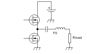
The two transistors are switched on and off by
two phase-opposed
square waves. The voltage at the mid point switches sharply between
ground and the supply voltage. A series resonant circuit at the output
offers high impedance to all harmonics, while conducting the
fundamental signal to the load. So the current flowing in each
transistor is a half sine wave, while the voltage is a square wave.
A transformer or tuned matching network can be inserted between the
resonant circuit and the load, to match to the desired load
resistance.
This particular configuration is extremely common in switching power
supplies operating at frequencies between 20kHz and maybe
1MHz,
and even a little beyond. But at HF it's hard to implement, because the
upper transistor needs to be driven relative to its source, which isn't
grounded, but instead swings up and down all the way between the
supply voltage and ground. Driving such a configuration at tens of MHz
incurs in some severe trouble with stray capacitances, and also
most transistors suitable for such frequencies come in casing styles
intended to be operated with a grounded source.
So, an alternative configuration has more chances of being successful
at RF:
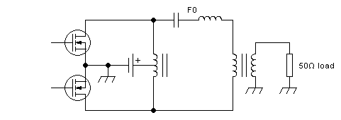
Here it is again - the good old push-pull circuit. In this incarnation
it has coupled drains, and a series-resonant circuit inserted somewhere
in the load circuit. If inserted between the transistors and the
transformer, like shown here, the transformer only sees the fundamental
frequency. If instead the resonant circuit is inserted after the
transformer, it's easier to band-switch, but then the transformer will
be exposed to the full harmonic frequency voltage, and this requires
the transformer to be designed to handle that, both in terms of core
loss and stray capacitances.
In this configuration the transistors switch their drains between
ground and off, and while off, the coupling in the bifiliar feed
transformer makes the drain voltage rise to twice the supply voltage.
The drain current conducted by each transistor is a half sine, defined
by the resonant circuit. The supply current is a rectified sine.
Instead of a series resonant circuit, it's possible to use a
series-input low pass filter. This could allow building a pre-tuned
bandswitched
amplifier. But the big problem with this configuration is achieving
good drain-drain coupling in the bifiliar feed transformer. It has to
be good all the way to pretty high harmonics! And that, my dear
readers, just can't be achieved in high power amplifiers. Take my word
for it, or try it yourself. Let me know if you have success. The higher
the power level, the lower is the frequency limit.
And this brings us to current-switching class D amplifiers. These
actually need
separate RF chokes that conduct a constant current over the RF cycle,
and they need
the drains being completely decoupled from each other! So,
using
current-mode class D turns a very difficult design problem into a very
easily implemented design feature!
Such a current-switching class D amplifier's output section might look
like this:
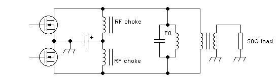
Like in the previous case, each transistor switches its drain between
ground and off. While at ground, it conducts the total supply current,
equal to the sum of both RF choke's currents, and constant throughout
the RF cycle. While off, the parallel resonant circuit forces the
drain voltage to be a half sine, starting from ground, not
from
the supply voltage. Assuming perfect transistors that have zero
saturation current and instantaneous switching, the voltage across the
RF choke on the side where the transistor is on, is the supply
voltage. Since that voltage is constant during the half cycle, the
peak, average and RMS voltages are all the same. While that transistor
is off, the RF choke must restore its DC balance, by forcing an average
voltage during the other half cycle that's also equal to the supply
voltage. So the half sine voltage at the drain will have an average
value of twice the supply voltage, starting from ground, and for a sine
wave this is an RMS voltage of 2.22 times the supply voltage, and a
peak
voltage of 3.14 times the supply voltage! This is a very important point to
be aware of!
While in well-implemented class A, AB, B linear amplifiers, and also in
voltage-switching class D amplifiers, the transistors only ever see
drain
peak voltages of twice the supply voltage under normal operating
conditions, in a current-switching class D amplifier they see 3.14
times the supply voltage, with perfect components, and roughly 2.8 to 3
times the supply voltage in a typical real-world implementation. So, a
transistor rated for 50V supply voltage, and 125V absolute maximum
drain voltage, is fine to be used at 50V in true class AB, but
in
current-switching class D it should be operated at only 33V to get the
same
reliability. Operating at 50V in current switching class D it will
produce much more power output than in true class AB, but at the cost
of much higher peak drain voltage that might well exceed the
transistor's absolute maximum rating, and destroy the
transistor!
I mention this so explicitly because many people trying to build class
AB amplifiers end up unknowingly building AB-D hybrids, due to poor
drain-drain
coupling, and kill transistors like crazy, without
understanding why the darn things blow up.
Instead of the parallel resonant circuit, this amplifier can be
operated with a parallel input (π configuration) lowpass filter. If
the filter is placed after the transformer, the full harmonic current
needs to go through the transformer. The voltage instead is close to a
sine wave, thanks to the filter, so the core sees no additional
stress from harmonic frequency voltage.
True class D amplifiers are usually operated with non-simultaneous
switching of the two transistors. To avoid shoot-through and the
corresponding high current pulse and loss, voltage-switching class D
amplifiers are normally driven in such a way that one transistor
switches off a small moment before the other one switches on. So there
is a brief "dead time", during which neither transistor conducts. If
this dead time is deliberately increased, the output amplitude gets
smaller. This is pulse width modulation, and is often used with
voltage-switching class D amplifiers at low frequencies, such as in
power supplies and audio amplifiers (including modulators). In fact PWM
is so common that some people think that voltage-switching class D is
necessarily tied to PWM. But this is incorrect. It's perfectly possible
to use voltage switching class D without PWM.
Current-switching class D amplifiers instead need to be operated the
other way around: Each transistor has to be switched off a little
later, not earlier, than the other one is switched on, in order to
avoid
generating a huge drain voltage spike during crossover, because if
there was dead time, the RF chokes would be forcing current into the
amplifier, that has nowhere to go. So the drive is arranged in such a
way that during
crossover both transistors conduct at the same time, and the RF
chokes keep the current at the normal value.
In RF amplifiers it's not possible to get absolutely true class D
operation, because transistors just don't switch instantly, and the
switching time even of UHF transistors is still significant at HF. We
can get close to true class D when using UHF transistors on the 160m
band, but only close, not fully there. So, in real-life class D
RF amplifiers, we never have precise square waves, but instead the
current has
a trapezoidal waveform with rounded corners. And we rarely get any true
clean voltage sine wave, but only something resembling a sine
wave, with obvious waveform distortion.
If the filter is placed after the transformer, there could very well be
a significant delay between the transistors and the filter, and this
causes
the reflected harmonic components to be out of phase with the
fundamental. As a result it often happens that on some bands we see an
approximate square wave on the drains, but on other bands
this changes into something closer to a triangle wave, or some other
peaky shape. It's not that
the harmonic structure has changed. Just the phase relations have
changed! But
this inconvenient phasing of the harmonic reflections can make the peak
drain voltage higher than 3.14 times the supply voltage... and that's
bad news for the transistors, and often explains why an amplifier that
worked well for years on several bands blows up instantly when tried on
a new band. A diplexer filter solves this by not reflecting any
harmonics. The drain voltage waveform will then become trapezoidal. But
since then the amplifier will produce significant power at harmonic
frequencies, and this power will be absorbed in a dummy load placed at
the diplexer's highpass output, the efficiency of such an amplifier is
poor for a class D amplifier, making the approach rather pointless.
Linear class D amplifiers
If a current-switching class D amplifier is driven with a square wave
of variable amplitude, then the two transistors will also conduct a
square wave of variable amplitude, instead of saturating. The resulting
amplifier output is a squarewave current, or in practical RF amplifiers
more like a trapezoidal current, whose amplitude follows the drive
signal. A capacitor-input low pass filter will force the
voltage
at its input to be roughly sinusoidal, and will largely eliminate
harmonics from the output. So the configuration of this amplifier's
output section is just like that of a current-mode class D amplifier
operated in saturation, but it is capable of linear operation simply
thanks to the driving scheme used.
And this, folks, is very important, because this is how many, if not
most broadband push-pull linear HF amplifiers work! Most people
believe them to operate in class AB, and are shocked when they see the
waveforms present inside such an amplifier. But really these are linear
class D amplifiers, and then the waveforms make sense!
To avoid shocking my dear readers too deeply, I'm willing to consider
all those 13V, 100W push-pull amplifiers, that we have used in millions
of radios since the 1970's, to be hybrid class AB-D amplifiers. But
they
are not
true class AB linear amplifiers as Adam described them, even if widely
publicized as such!
Such an amplifier's bare-bones output section typically looks
like this:
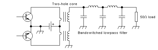
It uses an output transformer made on a two-hole core, with a
single-turn primary fed at the midpoint. Since such a transformer has
no magnetic coupling whatsoever between the two halves of the primary,
I drew it as two separate transformers, connected in series. It behaves
exactly like having two separate RF chokes followed by a simple
transformer. That is, it provides no coupling between the collectors.
This circuit has been implemented with BJTs for about 40 years, and
only later MOSFET versions appeared, which typically have some
differences. BJTs allow a very simple trick with biasing and driving,
to run them in linear class D. I will come to it in the chapter about
biasing.
Most amplifiers in HF communications are used in SSB mode. The
peak-to-average ratio in SSB is very high, so that an amplifier
designed for 100W PEP will in average be producing only 20W or less
output. A practical, well-implemented class AB amplifier might produce
65% efficiency at full power output, but at 20W it will be dramatically
worse, and over the entire SSB cycle too. For this reason some linear
class D amplifiers use a trick to improve the part-power efficiency.
This trick is to partially
couple the drains together, to achieve an
operation mode that lies halfways between class AB and
current-switching class D.
This efficiency tuning is most commonly done like this:
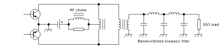
The bifiliar feed transformer would couple the drains together, if it
had its midpoint at RF ground. But the RF choke lifts it from ground,
and the resistor "partially grounds" it through the supply. The
resistance value controls the amount of coupling between the
collectors.
The resistor can also be connected from the bifiliar feed transformer's
midpoint to ground, via a DC-blocking capacitor. But connecting the
resistor across the RF choke is usually more convenient.
Back in 1977, Frederick Raab published the mathematical theory behind
this optimization in the IEEE Journal of Solid-State Circuits, calling
this configuration the "Class BD High Efficiency RF Power Amplifier".
And now in 2020, and many million such amplifiers later, still many
builders of RF amplifiers don't recognize
it even when they are pushed with their noses into it!
Designing those pesky transformers:
In recent years many designers and experimenters have been building
high power HF amplifiers using gemini-encapsulated MOSFET pairs such as
the BLF188XR, either single or in pairs. To help those experimenters,
here is some detail about the design process for that specific case.
The first step is deciding how hard we can load such a transistor. The
datasheet states that the RDS(on) is typically 0.08Ω at 25°C. It rises
with temperature, so at normal operating temperature it might be
roughly 0.13Ω. And this is the value when the gate voltage is driving
the MOSFET "fully on". The saturation isn't a knife-sharp process, and
thus the practical saturation voltage in linear RF power operation is
somewhat higher than the RDS(on) value would suggest. So, if we want to
avoid an excessively severe efficiency reduction due to
imperfect
saturation of the transistor, we need to keep the drain load
resistance above 1.3Ω or so.
In a push-pull circuit the drain load resistance on the transistor
that is on at a given time is one quarter of the drain-to-drain load
resistance. Some people stumble over this, and they believe that it
should be half the drain-to-drain load resistance. That would
be true if both transistors were on and working at the same time, such
as in a class A
amplifier. But not in AB, nor in class D. And those are the
classes we can use with such a large transistor. So it follows that we
want a drain-to-drain load resistance of at least 5.2Ω. If it is
higher, the efficiency will be better, but the power output for a given
supply voltage will be lower.
The impedance transformation ratios we can easily implement are 1:1,
1:4, 1:9, 1:16, perhaps even 1:25, corresponding to turns
ratios of 1:1, 1:2, 1:3, 1:4 and 1:5. Since we usually want to match to
a 50Ω load, a 1:9 transformer is the only reasonable choice, giving
5.56Ω drain-to-drain load. A 1:4 transformer would produce far lower
output power than the transistor is capable of, while a 1:16
transformer would result in a very inefficient amplifier that needs a
relatively low supply voltage in order to keep the dissipation
manageable. So, 1:9 it is.
Should we use a conventional transformer, or a transmission line
transformer? Let's try both, as a design exercise, and also to see
which one
has what advantages.
The first approach a typical designer tries is a conventional
transformer using two ferrite tubes (sleeves, large beads), side by
side, with a single-turn primary made from two little pieces of tubing
and sheet metal or PCB end plates, and 3 turns of wire wound through
the tubes to form the secondary. And the first questions that arise
are: How large do the cores need to be, and what ferrite material can
be used?
The core needs to fullfill at least two, and sometimes three
requirements:
1: The single turn must provide enough inductance for operation on the
lowest desired frequency.
2: The losses in the core must remain manageable, at the voltage the
transformer operates at, throughout the entire frequency range.
3: If the power supply is applied to the (false) center tap of
this primary, the cores need to stay well out of saturation, and inside
their linear ranges, when the highest expected DC current flows. This
requirement can be dropped if another feed method is used.
The minimum inductance required is a bit subject to negotiation. We
might want it to be so high that it has negligible effect on circuit
operation. That would be about 10 times the load on the winding. In
this case, the single-turn winding operating into 5.56Ω, the inductance
would need to have a reactance of at least 55.6Ω at the minimum
operating frequency. If we want the amplifier to operate from the 160m
band upwards, that minimum frequency is 1.8MHz, and the minimum
inductance is then 4.9µH.
If this turns out hard to implement, we can start to negotiate. At half
that inductance value, there will be some impact on performance on the
lowest band, but not much, so we might just accept 2.5µH as a minimum
value. And we can go even lower, if we compensate the transformer for
low frequencies! This is done by inserting properly calculated
capacitors in series with the primary and secondary, so that they form
a T highpass filter with the transformer's inductance. Since
the
capacitor on the primary side will block DC, this method can only be
applied if the supply current is not applied through the
transformer. And we
need to keep the cutoff frequency of this highpass filter well below
1.8MHz. This method allows us to get by with a primary inductance as
low as 0.5µH! This would require a 33nF compensation capacitor in
series with the primary, and a 3.6nF capacitor in series with the
secondary. Some people see such capacitors in a schematic
diagram and
scratch their heads about why they are there, given that there is no
need
to block any DC... Well, they are low-frequency compensation
capacitors, not DC-blocking capacitors!
You can use filter design software to design such compensation
networks. "Filter Solutions", from Nuhertz Technologies, works very
well and is very comprehensive. But much simpler software, online
calculators, or even just the plain equations obtained from textbooks
or the web, will also do the job.
There is a catch, though: If the transformer's inductance is so low
that we need to compensate it in this way, then the transformer will
operate at increased voltage on the lowest band, and this will increase
the core loss!
So, to round up the primary inductance requirement: If we can get 5µH
or so, that's plenty. 2.5µH is still OK. Lower values can be used, down
to 0.5µH, but require compensation and attention to increased core
heating. And if you don't need to operate on
160m, so that your amplifier has a minimum frequency of 3.5MHz, then
all these values can be halved.
The volumetric loss in a ferrite core depends in a nonlinear way mainly
on the
frequency, the volts per turn, and the core's cross-sectional area, and
the curves are specific to each particular material. The core's shape
also has some influence. So we cannot use
equations to calculate the loss, but have to look up tables or graphs.
Unfortunately it's very hard to find published loss data for ferrite
materials, applicable to the operating conditions in RF power
amplifiers. Ferrite manufacturers seem to shy away from publishing such
data, for whatever reason. So I measured the loss on several cores,
using home lab methods, and published the results in a web page
called Ferrite core loss in HF power applications.
Now the question is how much volumetric loss is acceptable. This
depends strongly on whether or not there is forced air cooling
available for the
transformer, and also on many other factors such as the size
of
the core (due to the Law of Sizes: Larger cores have more volume per
surface area than smaller ones), how much heat the windings generate,
what's the maximum
acceptable temperature for the ferrite and the wire insulation, and so
on. And the loss we need to consider is the average loss, so that in an
amplifier destined purely for low duty cycle modes such as SSB we can
use a much higher design value than in an amplifier intended for 100%
duty cycle. So I cannot give you a simple, fixed value for acceptable
volumetric loss. Just some very rough guidelines: For large cores like
the ones we need in a high power amplifier, 200mW/cm³ is typically OK
with forced air cooling in continuous service, and with natural
convection cooling in intermittent SSB service. Smaller cores can be
driven to higher volumetric losses.
Now notice how steep the curves are! For example, taking the
first graph:
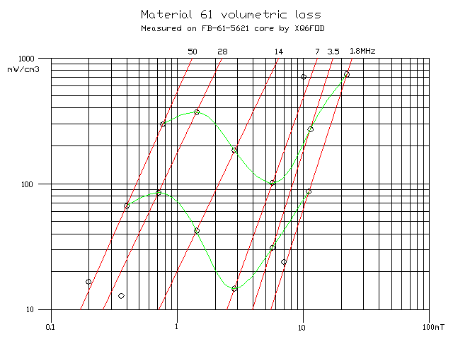
If you drive this material to a flux density of 10mT at 1.8MHz, the
loss is so low that the core might pass for "cold" when you touch it,
even on
the worst band, 160m. If you double the flux density to 20mT, the loss
becomes roughly 9 times larger, and unacceptable unless perhaps if you
use
low duty cycle and
forced air
cooling! So, despite the uncertainty we typically have in how much core
loss is acceptable, looking at these loss graphs we can get a pretty
good idea of what flux density we can use. In case of doubt, choosing a
slightly lower flux density will make the loss drop a lot and give us
headroom.
Note that with all RF-rated ferrite materials I measured, the highest
loss occurs at the lowest frequency, when the core is driven at
constant voltage from 1.8 to 54MHz, as is the case with typical ham RF
power amplifiers. But some
materials show a steady drop in loss toward higher frequencies, while
other materials, such as Fair Rite 61, have rather
idiosyncratic loss
curves. The green curves in my graphs show loss at constant voltage
excitation. With any RF ferrite, we need to calculate both the loss and
the inductance for the lowest frequency, and the rest of the frequency
range will be fine. But this is not true if you try to press
low-frequency ferrite material into RF use!
So, looking at this graph, you can see that when using material 61 and
designing for a flux density of 10mT at 1.8MHz will produce a
low-core-loss transformer, while 15mT might be the sweet spot between
core size and losses, and 20mT might be the absolute reasonable limit.
If instead you use material 43, you need to design for
slightly
lower flux density, roughly between 7 and 15mT for the same
range
of volumetric loss. And material 31 is very close to 43, in this
regard, just a tad better. If you use materials that I didn't measure,
you need to find loss curves somewhere else. Good luck with that! You
will probably have to measure the loss yourself. At least by making a
practical test of how much drive your core can take at the lowest
frequency, with acceptable heat rise.
Now let's start the maths. The BLF188XR has an
absolute maximum drain voltage of 135V. So, whatever
class
your amplifier operates in, you need to set the supply voltage such
that
this is never exceeded. And for safety reasons, you should stay
somewhat below it. So, 100V peak is fine, and we can design for this
voltage, because it doesn't matter if the transformer heats up under
conditions that anyway destroy your MOSFET! In true class AB, you get
100V peak with a supply voltage around 53V, and in
current-switching class D you get it roughly with a 36V supply.
100V peak is 71V RMS, if we
have a sine wave on the drains, which is what we should have both in
class AB and current-switching class D, which are the main classes for
such an amplifier. The required core cross-sectional area, for 71V RMS
across a single turn, at 1.8MHz, for 15mT flux density, is:
71V ÷ 4.44 ÷ 1800000Hz ÷ 0.015T = 0.00059m²
You can look up the equations in my article Transformers and Coils, and
apply algebraic transformations to them as needed.
As you can see, everything is in basic units. Afterwards of course we
can convert to more practical sub-units, and say that the minimum
required cross-sectional area is 5.9cm². This would give us operation
around the "sweet spot" with 61 ferrite, and hot-but-perhaps-managable
operation with materials 43 or 31. With slightly larger cross-sectional
area, materials 43 or 31 would work roughly at their sweet spots.
Amidon 1020-size beads are about the largest cores one can easily
obtain at reasonable cost. Not only from Amidon but also from other
distributors and made by other companies tha Fair Rite. These
beads measure roughly 26mm outer diameter, 13mm inner diameter, and
28mm length. So they have a cross-sectional area of 1.82cm². Two of
them side-by-side are definitely not enough to fulfill our requirement,
but using 4 of these cores gives us about 7.3cm², which would give low
loss with material 61, and acceptable loss with materials 43 or 31.
Just how much loss? The flux density at 71V RMS would be around 12mT at
1.8MHz. With material 61, and according to my measurements on
that
specific core type and size, this gives a volumetric loss of roughly
100mW/cm³ at 1.8MHz and almost the same loss at 54MHz, slightly less at
28MHz, and much less on all other bands. The volume of a 1020-size bead
is roughly 11cm³, so each bead would lose 1.1W, and the core loss for
the entire transformer would be 4.4W on the worst-case bands. With 43
material instead, the loss would be roughly 3 times as high, for 13W or
so of total loss. It would certainly need forced-air cooling if used
with a high duty cycle!
1020-size beads have rather large holes for such a
transformer.
Let's try beads with smaller holes, such as the Amidon 5621 size. These
are the same length as the 1020 size, but with an outer diameter of
14.3mm and an inner diameter of 6.3mm. So their cross-sectional area is
1.12cm². Six of these would be needed to get enough total
cross-sectional area. It would be 6.7cm², about 10% less than with four
1020 beads. This would make the flux density about 10% higher.
According to the measurement I did on that exact core, in 61 material,
it would result in a loss of roughly 150mW/cm³. Given that core volume
for each of these beads is 3.6cm³, and we have six of them for a total
volume of 21.7cm³, the loss on 1.8MHz would be arond 3.3W. So, despite
having a slightly smaller total cross-sectional area, and thus a higher
volumetric loss, the smaller total volume gives us a net improvement in
total power loss! But the dissipation surface is also much smaller, and
so these cores will get warmer. With 61 material the heating is still
low, but with 43 material it might start to become problematic,
depending on the duty cycle at which the amplifier runs.
The 5621 cores also have a cost advantage, since six of these are
cheaper than four of the larger ones.
The secondary consists of 3 turns of insulated wire looped through the
primary. For best coupling the wire should be as thick as fits in the
available space. With the 1020-size cores this results in very thick
wire, and would have to be implemented using coax cable, using the
shield as the conductor, to avoid having a massive, excessively stiff
conductor. With the 5621-size beads instead a normal sized wire can be
used. Teflon insulation is desirable, because it's highly
heat-resistant.
Now let's calculate the inductance. The inductance of a perfect cored
inductor is
Inductance = 0.000001257 × permeability × turns² × cross section area ÷
path length
where everything is in base units (inductance in henry, cross section
area in meters squared, path length in meters). We can cancel out a lot
of zeroes by expressing the equation in microhenries, cross-sectional
area in cm² and path length in cm, and rewrite the equation for
practical work in the quick and dirty way:
µH = 0.01257 × permeability × turns² × cm² ÷ cm
This equation assumes that all of the flux is in the core. But in
reality there is always also some flux in the air around, so the actual
inductance is a little higher. When using cores having very low
permeability this inaccuracy becomes significant, but not with
permeabilty 125.
The mean magnetic path length of a 1020-size core is 5.65cm. So, if we
make the
transformer using four FB-61-1020 beads, we get that path length, the
total cross-sectional area of 7.3cm², and with the
permeability
of the 61 material being 125, our single-turn primary gives us
an inductance of 2µH. This is in a range where at 1.8MHz we
will
notice some effect from lack of inductance but with some goodwill it
should still be
usable... If we use low frequency compensation, it's easy to
compensate for this inductance and get a flat response to well
below 1.8MHz.
To get a flat response on the lowest band without needing compensation,
you might consider using material 43. Thanks to its permeability of
850, this material would give us a primary inductance of 13.8µH - but
only at very low frequencies, far below the 1.8MHz point for which we
are
calculating! You need to be aware of this: The initial permeability
stated for a ferrite material is valid at very low frequency, and
beyond some higher frequency it starts falling off. For 61 material
this fall-off happens above roughly 30MHz, but for material 43 it
starts at a few hundred kHz! At 1.8MHz, the permeability is down to
roughly 500. So in fact we will only get roughly 8µH at 1.8MHz - which
is still plenty, and 4 times as high as with material 61.
Material 31 has an initial permeability of 1500, and at 1.8MHz it still
has about 1200. So with four FB-31-1020 beads we would get
close to 20µH, which is not just plenty, but far more than makes sense.
It's good to look at the manufacturer-provided curves for complex
permeability, and understand them. But it's also good to realize that
these curves are valid only at low flux density, and they
change
somewhat with the higher flux density used in power amplifiers. So they
don't tell the whole story for our purposes.
Let's do the same exercise for the six FB-61-5621 cores: 6.7cm² of
total cross-sectional area, 3.2cm mean path length, permeability 125.
We get 3.3µH, much better than the 2µH provided by the fat cores, and
enough to use without compensation nor worries at 1.8MHz. Which proves
that bigger
isn't always better! Shape matters.
Many ferrite beads of different sizes have very roughly the same ratio
between outer and inner diameter. The consequence is that the
inductance they provide depends on their total length
and permeabilty, and is nearly independent from the bead's
diameter.
I won't calculate the inductance of six 5621 cores made of higher
permeability materials, because it would make no sense to use those
lossier materials when the less lossy material 61 can provide enough
inductance.
So far we have nailed the core loss, core heating, and the inductance.
Now let's see what happens if we feed the amplifier at the false center
tap of this single-turn primary. The cores at each side of the
transformer will see the DC current consumed by the transistor on that
side, which is of course half of the total current. We are applying 71V
RMS to a 5.56Ω load, so we have a load current of 12.77A RMS in the
load, for a power of about 900W. If the amplifier works in class AB,
with just enough idling current to correct cross-over
distortion, each transistor conducts close to a half
sine of
current of twice this value, during its active half cycle. That's
25.54A. During the other half cycle it doesn't conduct. The supply
current is then the DC value corresponding to a rectified sine of
25.54A RMS, and that's very close to 23A. This is of course a value
that does not include losses in the core and other components, the
feedback circuit, etc, so we need to consider a slightly larger supply
current, maybe 26A. We should also consider the possibility of higher
current due to some load mismatch. So let's take 15A per side as a
referential value, and see what happens.
The average flux density in a core is given by
Flux density = 0.000001257 × permeability × turns ×
current ÷ path length
where again everything is in base units: Tesla, ampere, meter. If you
want to get rid of some zeroes, you can express this in millitesla and
centimeter:
mT = 0.1257 × permeability × turns × ampere ÷ cm
Note that the cross-sectional area of the core has no effect on DC flux
density, since a larger area results in higher inductance, this results
in larger voltage while setting up the field, and this larger voltage
cancels out with the higher area. See my article about Transformers
and Coils
about this. There I explain that DC works just like AC in inductors,
and why. But for the practical work in RF power amplifiers, let's use
the all-inclusive equation above for flux density, to save
some work.
Okay... Applying this equation, it turns out that an
FB-61-1020
core having 5.65cm mean path length, with 15A flowing through it, will
run at an average flux density of about 42mT. Note that this
is
just the average flux density, though. This core has an inner diameter
of only half as much as its outer diameter. The path lengths along the
inside and outside surfaces have the same ratio, and for that reason
the flux density along its inner surface will be twice that along its
outer surface! So the highest DC-caused flux density, along the inner
surface of the core, will be roughly 59mT, and along the outer
surface it will only be half that much. The ratio between each of them
and
the mean value is given by √2, of course, since the ratio between
inside and outside diameter of this core is 2.
And the actual instantaneous flux density varies at the RF rate,
between the DC value plus or minus the RF value. So the peak
flux
density is the mean DC flux density plus the peak mean RF flux density
(12mT at 1.8MHz, our worst case), multiplied by the square root of the
diameter ratio. And that turns out to be 76mT, in this case.
76mT is a value at which material 61 is still pretty linear, so we are
fine with this design. The FB-61-1020 cores can take the supply
current. But we don't have an enormous headroom, given that material
61 starts becoming nonlinear at roughly 120mT.
If we use the smaller FB-61-5621 beads, with their mean path length of
just 3.2cm, we get a mean DC flux density of 74mT, plus about 13.2mT RF
flux density, making 87.4mT peak flux density at the mean path length,
and given the diameter ratio of 2.27, the maximum peak flux
density along the inner surface is 132mT. This is a bit high. It would
probably still be acceptable, but this transformer would be running
pretty much at its absolute limit when also feeding the supply current
into the amplifier. It follows that when applying the power supply in
this way, it would be better to use the 1020 beads, to be on the safe
side.
And what happens if you want to use material 43? Well, using
FB-43-1020 beads, with their permeability of 850, the mean DC flux
density is 284mT! Add the 12mT coming from RF, multiply by √2 to get
the flux density along the inside, and the result is 418mT! But this
material becomes nonlinear at about 100mT, and is totally saturated at
300mT! So this isn't workable at all. If you put 15A of DC through an
FB-43-1020 bead, the inner zone of the cores will saturate, the
permeability drops
enormously, and the response gets very nonlinear.
With material 31 the situation is even worse, due to its even higher
permeability. The result is: If you want to run DC through a
single-turn primary winding, you are stuck to low-permeability ferrite!
Have you lost track?
What we have until here is that with four FB-61-1020 beads we
get
low loss, ample DC handling, while the inductance is a little
on
the short side for 1.8MHz operation but could be compensated if no DC
needs to be run through the transformer. So either you accept slightly
suboptimal performance at 1.8MHz, or you accept the need for
a separate feed system - but then you don't need these big
cores
anyway!
The six FB-61-5621 beads have even lower total loss, but warm up
slightly more due to their smaller dissipation surface. They provide
enough inductance on 1.8MHz, and could just barely handle the DC if
needed, subject to practical testing. This looks like a decent design
compromise.
43 and 31 material beads provide ample inductance, but are much more
lossy, and absolutely cannot handle the DC in this amplifier.
Of course there are lots of other core sizes, and when you look to
other manufacturers than Fair Rite there are several other suitable
materials, so you might want to do this evaluation for all cores you
can obtain. I would suggest to look specially for materials having
permeabilities between 200 and 400.
But let's not jump too happily to closing this chapter, because the
most problematic matter is still missing: What will be the highest
frequency at which each of these transformers can work well enough! The
big problem is that RF transformers have significant
leakage inductance, caused by imperfect coupling. Very simply, the
primary and secondary conductors do not occupy exactly the same
physical space, and so there is some magnetic field that encloses only
one of those conductors, and not the other. This creates inductance in
each winding that is not coupled to the other winding. This leakage
inductance appears in series with the transformer. Both windings have
leakage inductance, but for practical purposes it can be considered to
be on either side. The leakage inductance of the other winding is
transformed by the transformer's ratio to the side we are measuring on.
I don't have a good equation to calculate the leakage inductance.
Measuring it on such a transformer built with four 1020-size beads,
using thin wire for the secondary (about 1mm copper diameter), gives a
total leakage inductance of 440nH, as seen from the secondary side,
with a meter that uses a low testing frequency. At HF the
measured
leakage inductance should be slightly lower, due to stray capacitances
partially compensating it,
but the difference probably won't be much. Note that the leakage
inductance is independent from the core permeability. Even the complete
lack of a core won't change it!
With that leakage inductance, the transformer would produce decent
performance roughly up to 8MHz. Of course this is
unacceptable. It
is possible to compensate a transformer for high frequency by
absorbing the leakage inductance into a lowpass filter of a frequency
higher than the highest operating frequency. This is analogous to
low-frequency compensation, but the capacitors are added in parallel to
the windings, and thus they don't block the DC. The bad news
is
that with 440nH of leakage inductance on the 50Ω side, optimal
compensation flattens the frequency response only to about
20MHz.
At 30MHz it's already more than 1dB down, and please let's forget about
54MHz! It would be impossible to operate on the 50MHz band with this
transformer, even after compensation.
The coupling factor can be improved by using thicker wire for the
secondary, trying to fill out the primary tubes as much as possible.
The thickest wire of which I could pass three turns through my
thin-walled primary tubes was RG-58 coax cable. Using its braid as my
secondary
conductor, the leakage inductance dropped to 337nH. Better, but still
not brilliant. Using optimal compensation, this version would
be
entirely usable to 30MHz. The response is down about 0.3dB at
30MHz. But at 54MHz it's still unusable, with an attenuation of more
than 5dB! The required compensation capacitors are 67pF
across
the secondary winding, and 612pF across the primary.
Another way to build such a transformer is to forget the metal tubes,
and instead wind three turns of coax cable, then use the intact inner
conductor as the secondary, and cut up the outer cover and the braid so
as to connect the three loops of braid in parallel, to form the
primary. This causes a significant improvement in the coupling factor,
because the entire secondary conductor is completely surrounded by
primary conductor, centered in it, and each secondary turn doesn't
"see" the other secondary turns. I made a transformer in this style,
using the same RG-58 coax cable, and obtained 202nH leakage inductance,
as seen from the secondary side. Properly compensated, this transformer
might work well enough to 54MHz, the response being 0.45dB
down at
that frequency. The compensation capacitors are 40pF across
the
secondary and 364pF across the primary.
Since it was easy enough to do, I soldered a 39pF capacitor across the
primary, a 330pF and a 33pF capacitors to the secondary, and also 6
resistors of 33Ω each to the secondary. This implements the calculated
compensation, and a 5.5Ω load, with hopefully low series inductance.
Then I measured the response, using my recently acquired NanoVNA. This
is the reflection coefficient I obtained:
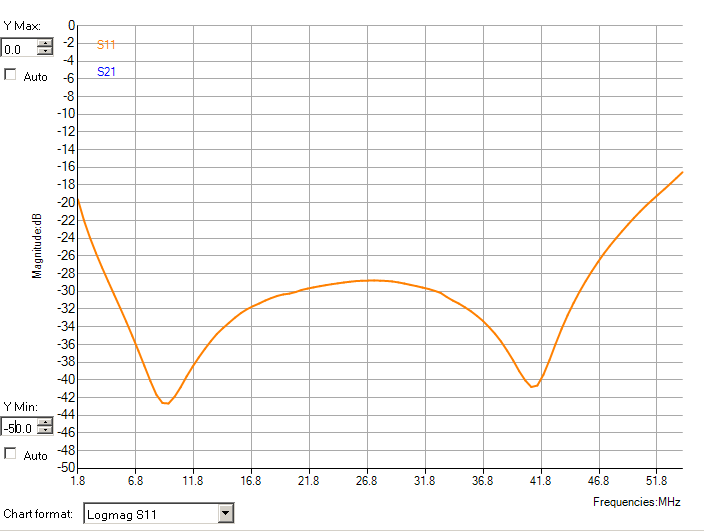
It's just like expected! The response at 1.8MHz is just at the
acceptable limit, which is usually considered to be a reflection of
-20dB.And at 54MHz it's a bit too bad. The reflection crosses -20dB at
50MHz and gets close to -16dB at 54MHz. Really we should try this with
coax cable having a lower impedance, thus getting a better coupling
factor!
To see what we have, here is the series impedance plot.
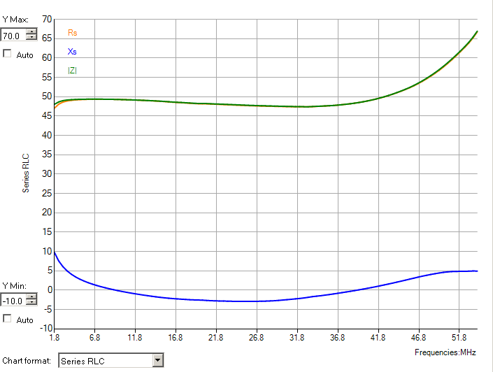
The resistance is a tad below 50Ω, simply because my 33Ω resistors are
also a tad low, and anyway six 33Ω resistors give 5.5Ω instead of
5.56Ω. Let's split some hairs, right? At the low frequency end we see
the effect of the main inductance of this transformer being just at the
acceptable limit for 1.8MHz, providing 10Ω of series reactance. This
could be corrected by adding series capacitors. From there up the
transformer works great, although around 30MHz the impedance
transformation is a tiny bit off, which could surely be corrected by
fine-tuning the compensation capacitances on both sides. But at the
high end the transformation ratio runs away, because we are nearing the
cutoff frequency of the compensation network. To fix this, we need to
further reduce the leakage inductance.
This could probably be done by using 25Ω coax cable. I don't
have any 25Ω coax cable at hand to cut up and try,
and I was too lazy to make any. But if I was making an amplifier of
this kind that has to operate to 54MHz, I would try this. Note that
since the braids of all turns are at the same potential, the outer
insulation could be completely removed, to save space and ease
the
splicing and soldering job. But in that case it would be good to use a
coax cable that has a very tight braid, so it won't separate much from
the dielectric.
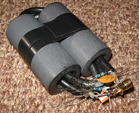 This is my test transformer. Neither tidy nor nice, but good enough to
test whether the stuff I'm writing here actually works!
This is my test transformer. Neither tidy nor nice, but good enough to
test whether the stuff I'm writing here actually works!
Of course such a transformer should use teflon-insulated coax cable,
due to its excellent heat resistance. And if I used it in an actual
amplifier, I would bring the coax solder points down to the board and
solder them there, so that good nice very wide copper areas can be used
to provide low impedance connections. In a practical amplifier the
drain connections will always have significant inductance, even if they
are just a rectangle of copper 10mm wide and 15mm long. It might be a
good idea to try compensating them too, by adding the required
additional capacitance to the transformer primary, and using the
transistor's output capacitance on the other side. This would require
clever dimensioning of the board traces.
Such a coax-wound transformer has input and output at the same end,
unless you are willing to do some more cutting and patching.
But
it's rather easy to accomodate this on a board.
I decided to also try a transformer made with six FB-61-5621 beads, in
two rows of three, side by side, with single turn copper pipe primary,
and three turns of the same wire used for the first experiment with the
four 1020-size beads. A slightly longer piece of the wire was
required, due to the longer turn length. The three turns of this wire
fit snugly in these cores. The leakage inductance, as measured
on
the secondary side, turned out to be 443nH, within 1% of what I got
with the larger cores! Obviously the advantage of better coupling, due
to filling out the primary tubes with the secondary, cancelled out with
the disadvantage of the greater turn length.
But with this small transformer there is not much to be gained with
thicker wire. At most one could use some wire that has a thicker
conductor and thinner insulation. And if winding coax cable on these
cores, miniature coax cable would have to be used, which can't handle
high enough power.
The primary inductance measured exactly 4µH, slightly better than the
calculated 3.3µH. This means that indeed the performance of this
transformer should be good at 1.8MHz. So I tested this transformer both
with and without compensation, to see if it is good for anything. Just
as a joke, I tried it first without any compensation, but with a nice,
precise 5.56Ω load. This is the series impedance graph, from 1.8 to
54MHz:
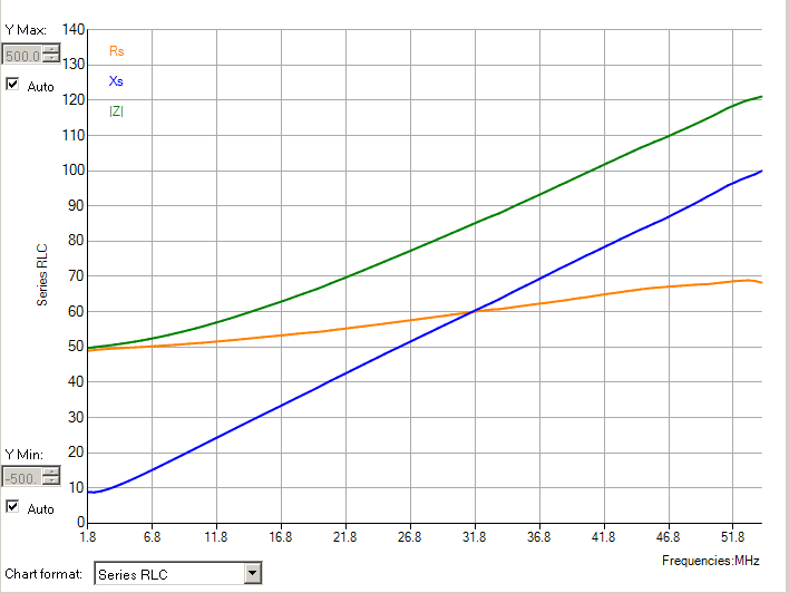
At least on the 160m band it's usable...! Maybe on 80 meters
too.
But beyond that, the leakage inductance kills it. So let's try
compensation. A 3-pole lowpass filter with its -3dB point
at 36MHz
can absorb the leakage inductance of this transformer. It needs an 88pF
capacitor across the secondary and a 792pF one across the
primary.
I soldered two 390pF capacitors across the secondary, and one 82pF
across the primary. This is the result:
 With
this compensation, the transformer would be fine
from 1.5MHz to 22MHz. That's the range in which the
reflection stays below -20dB. The reactance remains acceptable all the
way to 30MHz, but the transformation ratio deviates too much. I tried
to find better compensation capacitances by trial and error, but the
ones calculated from theory proved to be the best. So this
transformer isn't usable beyond the 15m band, and for that reason most
hams won't want it. Case 5621 closed! Posing for the photo at right was
the only thing this transformer was good for. Note that this test
transformer has primary and secondary connections on the same end, only
because I'm getting old and a tad stupid, and such things happen... Of
course I would wind it with the connections on opposite ends if it was
to be used for real. That would be more practical for board layout.
With
this compensation, the transformer would be fine
from 1.5MHz to 22MHz. That's the range in which the
reflection stays below -20dB. The reactance remains acceptable all the
way to 30MHz, but the transformation ratio deviates too much. I tried
to find better compensation capacitances by trial and error, but the
ones calculated from theory proved to be the best. So this
transformer isn't usable beyond the 15m band, and for that reason most
hams won't want it. Case 5621 closed! Posing for the photo at right was
the only thing this transformer was good for. Note that this test
transformer has primary and secondary connections on the same end, only
because I'm getting old and a tad stupid, and such things happen... Of
course I would wind it with the connections on opposite ends if it was
to be used for real. That would be more practical for board layout.
After this failed attempt, it would be logical to go to the other
extreme now, and try a particularly short and fat set of cores, that
achives the shortest possible turn length per core cross-sectional
area. This would minimize the leakage inductance, but at the same time
would increase any trouble coming from unequal flux density
distribution in the cores. It would also require a larger total ferrite
volumen, increasing weight, cost, and total core loss.
The best core shapes for such a transformer would be RM cores, or pot
cores. You would need something like an RM28 core (28mm center leg
diameter), made from an RF-capable ferrite. A permeability between 120
and 200 should be optimal. Good luck finding any! We can dream, right?
Since we can't wind a transformer on a core we can't get, our best
chance would be extra large beads. Amidon sells some jumbo beads in
materials 43 and 31, but unfortunately not in 61. When using such large
cores of the lossier materials, we need to use some extra
cross-sectional area to keep the flux density low enough to get
acceptable
loss. Just for the fun of it, I will make a design exercise with two
Amidon FB-43-20003 beads. Each of these has an outer diameter of
50.8mm, inner diameter of 25.4mm, and a length of 38.1mm. Yes, American
company, inch sizes... Let's round the dimensions to 51, 25
and 38mm.
Two of these beads will have a cross-sectional area of
9.5cm²,
and the turns shape will be close to a square, which is the next best
we can get after a circle. The average turn length will be about 20cm.
And that's already a tad more than the four 1020-size beads need, so
the leakage inductance would be worse! The only way to achieve an
advantage might be to stay far away from filling the whole big holes of
these cores with wire, and wind tighly with the shortest turn length
possible. Three turns of RG-58-size coax cable should end up having a
turn length of about 16cm. That would give a very
slight
advantage over the four 1020 beads.
The average flux density at 1.8MHz would be around 9mT, so the
volumetric core loss would be around 150mT/cm³. But the total core
volume is 118cm³, so we would get close to 18W core loss, at
full
power output and 1.8MHz! At this point the approach stops looking
attractive.
If you can find beads or toroids made of low loss material, in a
permeability range of 200 to 400 or so, that can be stacked in
such a way as to obtain 6 to 8cm² total cross-sectional area,
with
a
round or nearly square winding loop shape, it would be worthwhile to
make a design exercise with them. Otherwise just use the four
FB-61-1020! Or perhaps look for any core combination that are stacks up
a little longer than these. Properly compensated at the high
end,
they would produce very flat 1.8 to 30MHz response, instead of the
roughly 2.3 to 42MHz very flat response of the four FB-61-1020.
Toroids?
Instead of using a single turn primary on a fat core, it is
theoretically also possible to use a multiturn primary on a thinner
core. The result is usually a longer winding, and thus more leakage
inductance, but on the other hand the main inductance is also larger.
Just to see what happens, let's consider using a single big toroid and
design this transformer on it. I will choose the very well known Amidon
FT-240-61. It has a cross-sectional area of 1.6cm² and a mean path
length of 15cm. Its cross section is square with slightly
rounded corners, pretty much the best we can obtain.
At the RF operating voltage it gets in our amplifier, a 4-turn
primary will produce a flux density of 13.9mT at 1.8MHz, which is fine.
This means that the secondary needs 12 turns. And a bonus is that we
can make a real center tap on the primary, since it has an even number
of turns, and this allows us to feed the amplifier through this true
center tap, allowing us to operate in true class AB. As long as the
amplifier is well balanced, the DC in the primary turns will
cause
opposite fields and thus create no flux in the core.
The problem is that we can't just wind 12 turns of wire on this toroid
for the secondary, and then wind 2+2 turns of a wide conductor (braid,
metal tape) over it, because the coupling factor would be absolutely
terrible! Just for the sake of a laugh, I did it. I got
2.1µH leakage inductance, as seen from the secondary side! It
would be
possible to reduce this somewhat by tidy construction, but not a lot.
So this simplistic approach is a no-go.
It would be possible to do better by twisting three enameled wires
closely together, and then make six windings of two turns each. These
windings can each sit at one part of the toroid, they don't need to
overlap. Then all 36 wire ends need to be freed of their enamel
insulation, and interconnected in such a way that one wire from each
trio forms the secondary, with all six of them connected in series,
while another wire from each trio forms one side of
the primary,
all six of them connected in parallel, and likewise the last wire from
each trio form the other side of the primary. All interconnections need
to be made extremely short, to avoid introducing more leakage
inductance than what's inevitable.
With a core this size, I don't think that the result could compete in
terms of leakage inductance with the coax winding on beads described
above. And if it was messy to peel, cut and interconnect those coax
cables, it's far more messy to scrape away the insulation of 36 very
short ends of enameled wire, and then correctly (!) interconnect those
36 wire ends. It would require an amplifier masoquist to do
that.
Anyway the primary inductance of this approach is about 2.6µH.
Somewhat better than the four 1020 beads, OK for 1.8MHz, without any
excess.
So the bottom line is that the best conventional transformer I can come
up with, for this amplifier, is three turns of teflon coax cable,
probably of 25Ω impedance, wound through four FB-61-1020 beads, using
the shields as primary and the inner conductor as secondary. It gives
barely enough inductance on 1.8MHz, could easily be compensated to have
flat response to a lower frequency, and with 25Ω cable and optimal
compensation it would very likely be good enough to 54MHz. It's
reasonably easy to make, too. It can handle the DC, if the builder
choses to feed the amplifier through the false center tap of this
transformer (at the midpoint of all three shields), but of course this
is acceptable only for class A and current-switching class D
amplifiers, and since nobody in his sane mind would build a class A
amplifier around a kilowatt-class transistor, that only leaves class D.
For class AB a separate bifiliar feed choke is needed, that couples the
drains.
Transmission line
transformer calculation:
Let's now see how to design transmission line transformers. First we
will look at the 1:9 true, equal-phase transmission line
transformer, that doesn't need a separate balun. To refresh your mind,
I mean the transformer in this circuit:
The three transmission lines are identical in impedance and length. The
impedance must be one third of the 50Ω load, and three times the 5.56Ω
they present on the input. This is a direct consequence of the lines
being connected in series at the load, and in parallel at the input.
The lines do not perform any impedance transformation! They work at
their own impedance, front-to-end. The transformation is obtained just
by connecting them in parallel at one end and in series at the other
end.
So we need transmission lines having an impedance of 16.67Ω, or very
close to it. In theory the lines could be coax cable, parallel cable,
twisted wires, strips of double-sided flexible PCB, or whatever else
you can come up with, that fulfills the impedance requirement, and can
handle the voltage and current present in them. Of course, each line
works at the full input voltage, one third of the output voltage, and
at the full output current, one third of the input current. In this
design example that's 71V RMS and 4.3A RMS. The lines must be
able
to handle this over the full frequency range, without excessive loss.
Each line works at one third the output power, so roughly 300W.
There are very few companies that make such special
transmission
lines, they are hard to find, and absurdly expensive when
bought
in small quantities. So it's
better to make one's own lines. One can buy teflon-insulated
wire
in various sizes, and use braid harvested from cheap coax cables, to
make one's own coax cable in any desired impedance from about 10Ω to
100Ω. Parallel lines are easy to make from about 100Ω to 500Ω or so.
Coax lines below 10Ω can be made by making the inner conductor from
braid on a passive core, and using very thin insulation, for example
kapton tape. With any homemade coax line, after applying the outer
conductor one can apply shrink wrap to hold them together. There is
even teflon shrink wrap, which works at higher temperature, but is
expensive. One could also just wrap them with PVC electrical tape, for
testing and non-demanding low-temperature applications. There
are
online calculators to find out what diameter ratio is required,
depending on the desired impedance and on the dielectric material used.
These lines are wound on ferrite cores. For these cores the same
requirements and calculations apply as in the case of conventional
transformers: One needs to select a suitable core and turns number to
provide the required inductance at the lowest frequency, and keep the
flux density low enough to keep the core loss at an acceptable level.
So we need to know what voltages appear end-to-end on each line, and
how much inductance is necessary.
Let's calculate the voltages in a very simple way: Let's consider that
at a given instant the drain voltage of the upper transistor is at RF
potential "1". Then of course the bifiliar feed transformer forces that
the drain of the lower transistor is at RF potential -1. So all three
lines have their shields connected to -1, and their center conductors
connected to 1, and thus their inputs are in average at potential zero.
Each line has 2 between its center conductor and shield.
On the output side, the shield of the lowermost line is grounded
through a capacitor. So it is at potential zero. Since it has 2 between
its conductors, its output center conductor is at potential 2, and in
average the output is at 1. The mid line has its shield connected to 2,
so its center conductor is at 4, and in average its output is at 3. The
upper line has its shield at 4, so its center conductor is at 6, and in
average its output is at 5.
So, the lowermost line has 1 across it from end to end, the middle line
has 3, and the upper line has 5.
Since the RMS voltage between drains is 71V, our potential "1" in this
case equals 35.5V RMS. It follows that the lower line sees 35.5V
end-to-end, the middle line sees 106.5V, and the upper line sees
177.5V. And this means that the three lines need very
different minimum values for the ferrite cross-sectional area
×
turns number product. Since these are minimum requirements, it's the
designers choice whether to actually use different cores, different
turn numbers, or make all three identical and design them for the
requirement of the uppermost line. In the latter case, the cores of the
mid and lower lines will work at very low loss. Instead in the
former case, it's possible to save a significant amount of ferrite
(=cost, weight).
Since identical line lengths are required to keep the output signals
properly phase-aligned, a method that is very attractive is
using an
identical number of turns in each line, but different numbers or sizes
of cores.
In the example at hand, if we want to use 61-type ferrite and keep the
flux density below 15mT at 1.8MHz, at 177.5V we need a turns × area
product of 15cm² for the uppermost line. The middle line would be OK
with a turns × area product of 9cm², and the lowermost with just 3cm².
If we choose to wind each transmission line in 3 turns, we need cores
totalling 5cm² cross-sectional area for the uppermost line, 3cm² for
the middle line, and just 1cm² for the lowermost line. Or we could use
identical cores of 1cm², and wind 15 turns, 9 turns and 3 turns
respectively. In practice we need to see what cores are available,
consider their cross-sectional areas, their winding space, the diameter
of the transmission line used, and find out which is the most
convenient core and number of turns, in terms of cost, size and loss.
But while we do this, we must also make sure that we get enough
inductance.
How much inductance we need, depends on how much imbalance we can
tolerate. If we want perfect balance in the amplifier, we need
infinite inductance.
The input sides of our lines are RF-ground-referenced by the
amplifier's supply circuit. And the output side
is ground-referenced at the lowermost point, the shield of one line.
This confinement makes the lines work at the fixed end-to-end voltages
already mentioned, assuming 71V RMS drain-to-drain voltage. So the
common-mode currents they inject into the amplifier depend strictly on
these voltages and the end-to-end impedance of each line wound on its
core. It's good to think of impedance here, rather than reactance,
because many ferrites used in this application have a more resistive
than reactive behaviour in the upper part of the HF spectrum. But at
the lowest frequency, which is usually the worst case and thus the
frequency we have to design for, most RF ferrites are mostly
inductive, so you are allowed to think in terms of
reactance and inductance!
Very simply stated: The uppermost line in this example works at 177.5V
RMS end-to-end, and the unwanted common-mode current it injects into
the amplifier depends on this voltage, and its choking impedance, by
Ohm's Law. The big question is: How much of this unwanted common-mode
current is acceptable? There is no obvious, clear answer to this. It's
a design trade-off like so many others. We might want to keep this
common-mode current to one tenth of the total drain current, as a
simple rule of thumb. The smaller we make it, the better
balanced the
amplifier will be.
Not only the uppermost line injects unwanted common-mode current. The
others do it too, and in this transformer configuration, all three
common-mode currents are in the same phase, and thus add up. We need to
distribute the one-tenth allowance among those three lines, in a way
that is practical to implement.
If we intend to use the same number of turns for all three lines, and
vary the ferrite cross-sectional area in the ratio 1:3:5, then the
inductances will also vary in that ratio, and since the end-to-end
voltages have the same ratio, each line will contribute the same amount
of common-mode current. So we assign one third of the one tenth
allowance to each line. The total drain current in this example
amplifier is roughly 30A, so we will accept 1A of common-mode current
in each line. That requires a reactance of 177.5Ω for the uppermost
line, which at 1.8MHz is an inductance of 15.7µH. If we design the
uppermost line for this value or higher, and then scale the ferrite
cross-sectional area for the other lines, all will be fine.
To avoid ending up with enormous ferrite cores, it's a good idea to
start with the thinnest transmission line that has the proper
impedance and that can carry the required power over the full frequency
range.
Let's assume that for this application you were able to make a coax
line of 16.67Ω impedance, that can carry the required 300W,
and has
a diameter of 4mm. Then we start trying: The FB61-1020 core could
accept a maximum of 7 turns of this line. It gives roughly 0.5µH for
one turn. Inductance depends on the square of turns number, so 7 turns
gives roughly 25µH. Plenty enough! The ferrite cross-sectional area
times the turns number is roughly 12cm². But we need at least 15cm²!
Hmmm... We can't wind more turns, because they don't fit. So
we
need more ferrite, unless we can somehow shrink the coax cable to pass
two more turns through this core. That's why thin transmission line is
so important!
Assuming that we can't shrink the cable, the next attempt could be
using two FB-61-1020 beads side by side. Having twice the ferrite
cross-sectional area, 5 turns is enough in terms of flux density. It
gives us
roughly 12.5µH, and that's a bit low. But 6 turns on these two cores
would be fine for the upper line.
The middle transmission line is OK with three fifths the core
area × turns product, and inductance. Putting six turns on a single
core would give a tad less than that - but we have space for 7 turns!
So we use a single core, wind 7 turns on it, and call it a day. The
cable length required for 7 turns on a single core is very similar to
that required for 6 turns on two cores side-by-side. Of course, for the
sake of phase alignment, we should make all three lines identically
long. Any slack can be taken up by expanding the turns a little.
And the lowermost line would be OK with fewer turns or a slightly
smaller core, but why do it? It's more practical to use the same core
size throughout. And since anyway we need to use the same lengths of
transmission line, I would just make the lowest line identical to the
middle one, 7 turns on a single core. That core will work cold, while
the
other ones will get warm under the worst operating conditions.
So, we end up with a lot of practical compromises, and using a total of
four FB-61-1020 cores for this 1:9 transmission-line transformer. And
that's the same amount and type of ferrite we needed for the
conventional transformer! Funny, huh?
The lower frequency limit of this transformer is given by excessive
common-mode current injection into the amplifer, and we have set it by
design to 1.8MHz or slightly below. The upper frequency limit is given
mainly by inter-turn capacitance, which tends to short out the choking
effect and thus inject excessive common-mode current. In the
transformer described this capacitance will be just a few pF, maybe in
the low tens of pF, and depends on construction details, such as the
thickness and dielectric constant of the outer insulator of our coax
cable. We can use the transformer up to a frequency where this
capacitance has a reactance of the same 177.5Ω. For example, if we get
10pF total input-to-output capacitance, it limits the operation to a
maximum frequency of roughly 90MHz.
If we get too much capacitance for the highest operating frequency
desired, we can try reducing it by using a coax cable with thicker
outer insulator, made of low dielectric constant material (teflon),
also by avoiding packed windings (like in side-by-side cores) and
prefering windings airily distributed around a single core, with the
largest turn spacing possible. But the parts of the cable that
are inside
the core will still be very close together, and this can be eased by
using a large diameter toroid instead of a bead, and keeping some
distance between the first and the last turn. In extreme cases two or
more wound cores can be placed in series to form one transmission line
choke.
Since the three lines work at known end-to-end voltages, we can in
principle wind them on a single core. In that case we must
painstakingly follow the 1:3:5 turns ratio, and of course we must get
the phasing right, by winding them all in the same sense. But I don't
think it's a good idea to do it in this case, because we would need a
very large core to fit all those turns. Such a core is more expensive
than several small ones - if it exists at all! Also the capacitances
between turns become more of a problem. But with transmission-line
transformers used at low voltage and low power, core sharing is a
definite possibility.
Now let's do a design exercise for the other configuration:
The bootstrapped 1:9 transformer uses two lines of 16.7Ω. Since their
outputs are connected in series with the input signal, any phase lag
that happens along the lines is detrimental, and so these lines should
be as short as possible. Their length are the main factor defining the
upper frequency limit.
Like in the previous example, the input side of both lines have an
average
RF potential of zero, while their output sides have the shields
bootstrapped to the inputs, so the upper line has its output side
shield at "1", its center conductor at 3, and thus the average output
is at 2. The lower line is the same reversed, that is, its shield is
bootstrapped to -1, its center conductor is at -3, so its average
output is at -2. As a result both lines have identical end-to-end
voltage, although in reversed phases. This voltage is "2", and as
explained in the example above, this equals 71V in this amplifier.
The common-mode current in these lines appears as inductive loading
current on the amplifier. We want to keep it down to a total
of
one tenth the amplifier current, so we can allow about 1.5A per line at
the lowest frequency. That calls for a minimum reactance of about 47Ω
at the lowest frequency, which is 4.2µH for 1.8MHz.
Using the methods already explained, and trying our old friend the
FB-61-1020, four turns on one core are enough to handle the voltage.
They will give us around 8µH, which is also enough. Note that this
under-utilizes the 1020-size core. We could try to use a smaller core,
maybe two significantly smaller beads side-by-side, which saves a few
cents and also makes the design nicer to look at. Or we could keep the
1020 size beads, and have some headroom to use slightly thicker coax
cable.
This bootstrapped transformer is ideally suited to winding it on a
single core, due to its symmetrical operation of two identical lines
under identical stress. If you do so, don't forget that the two lines
work with opposed end-to-end voltage, so they have to be wound in
opposite senses on the shared core! But this too helps symmetrical
construction.
Remember that the best design for this transformer is the one that ends
up with the shortest lines. The total electrical length of each line
should stay below 8% or so of the wavelength, at the highest frequency
that will be used. If that's 54MHz, then the maximum allowable
electrical length is around 48cm, and if the cable has a velocity
factor of 66%, the maximum allowable physical length is just 32cm. This
is probably not yet a problem in this example, but may be close to the
limit.
If it does become a problem, there is a simple fix: Instead of making
the bootstrapping connections short and direct, they can be made with a
third transmission line, connected exactly like in the previous
example.
Since this line doesn't need to sustain any end-to-end voltage, it
doesn't need to be wound on a core. It's just a delay line. So, cut a
piece of your low impedance cable, the same length as the other two,
coil it up in the air, and use it for the bootstrap connections.
Problem fixed! The line length restriction is now removed, and the
upper frequency limit has been extended to whatever the stray
capacitances will allow. But at high frequencies, where this line alone
has significat end-to-end inductance, the output side of the 1:9
transformer becomes floating, instead of being referenced to the
amplifier's grounding, and this can cause imbalance between
the two main lines.
The output balun works at 50Ω at both sides, so it's wound with 50Ω
coax cable. This cable has to carry the full power, so we can't use
miniature coax. RG400 or similar is typically used. Its input side is
nominally at average potential zero, and its output at "3", so it sees
106.5V between its ends. The common-mode current it conducts will be
injected into the amplifier, so it has to be kept low. Applying the
same one-tenth rule of thumb as before, and considering it's just one
line injecting this current, 3A would be acceptable in the worst case.
So we need at least a reactance of 36Ω or so at the lowest frequency,
but more is always better in this case. At 1.8MHz that's a minimum of
3.2µH.
On a single FB-61-1020 we would need six turns, to satisfy the flux
density and loss requirement. But six turns of RG400 don't fit. So we
need to use two of those cores. 3 turns would give acceptable
flux density, along with 4.5µH, which is acceptable. But a fourth turn
can be wound, resulting in less core heating and much lower imbalance,
so that's what I would suggest.
Funny... Using one FB-61-1020 for each section of the 1:9
transformer, and two for the balun, again
we ended up with 4 of those cores! Isn't this spooky?
So, it's your free choice whether you use a conventional transformer, a
full 1:9 transmission-line transformer, or a bootstrapped 1:9 plus
balun. In all three cases you can use the same cores. Only the coax
cable
needed is different. But there are important differences in the
performance: The conventional transformer requires very careful
construction and compensation, to achieve just enough
performance.
Instead both transmission-line versions are easy to get right, and will
give a very flat response. That's why most builders of such amplifiers
prefer transmission-line transformers. But the transmission-line
transformer also has mighty disadvantages, where the conventional
transformer wins. One of these is the long delay of transmission-line
transformers. Their line, from input to output, might easily have an
electrical length of 100 to 150cm! This creates big trouble in
class D amplifiers. After all, they need
the
lowpass filter to define the waveform at the drains, either voltage
or current! If the lowpass filter is connected through a long line like
this, the
harmonics reflected by the filter arrive totally out of phase, and lead
to horrible and often dangerous waveforms at the drains, which are
totally different between one band and another. A current-switching
class-D amplifier needs a filter that essentially short-circuits the
harmonics. At any frequency where the delay between the drains and the
filter is a quarter wave, or an odd multiple of that, the
filter-provided short circuit will be transformed by the line into an
open circuit, leading to immense drain voltage spikes that kill
transistors like flies. And if we have 100cm of electrical line length
there, the lowest frequency where that will happen is 75MHz, the third
harmonic of our 12m band, and close enough to the 5th
harmonic of our 20m band. Longer line lengths make the problem start at
even lower frequencies. And even on frequencies where the line is
shorter than a quarter wave but still of significant length,
it causes impedance transformation, turning the short-circuit
reflection from the lowpass filter into a nasty inductive load.
Conventional transformers cause less delay, and what delay
they do
cause, happens because of their leakage inductance, that has to be
compensated by absorbing it into a lowpass filter - and the input
capacitor of this filter
then provides the required near-shorting of harmonics, on the higher
bands! This is why conventional transformers are preferable in
class D amplifiers. People who build class D amplifiers with
transmission-line transfomers often see themselves forced to use a
diplexer filter instead of a plain lowpass filter, to absorb the
harmonics rather than reflecting them, and have to accept the higher
filter complexity and a significant efficiency reduction.
And don't say that this is irrelevant to you because you are building a
class AB amplifier, not class D. The bad news is that if you are
building a kilowatt-class 50V-powered amplifer, it will
operate in a mode close to current-switching class D, at least
on
the higher bands, whether you want it or not! I will come to this a
little down this page, when looking at feed transformers...
Another advantage of conventional transformers is that they provide the
required DC blocking. This might seem minor, since two little
capacitors are cheap and easy to add, but it is important if the
amplifier will be modulated through the supply voltage. In that case
any coupling capacitor ends up loading the modulator. A typical
modulator is a class D amplifier operating with PWM at a carrier
frequency around 200kHz, and has a carefully designed lowpass filter at
its output to reject the 200kHz switching frequency while passing the
modulation frequencies, which might extend to 30 or even 50kHz, for
clean SSB operation. This filter would be totally upset if
RF coupling capacitors were added to the RF
amplifier! Any
capacitance in the amplifier's drain circuit needs to be absorbed
into the modulator's lowpass filter's design, and
there is a
limit as to how much capacitance can be absorbed. That makes a
conventional transformer highly
attractive for such envelope-modulated amplifiers.
Finally a conventional transformer has the advantage of needing less
coax cable, of less critical impedances, and in less demanding cases
it can be wound with plain wire, and it is more compact.
The conventional transformer and also both versions of the transmission
line transformer allow injecting the DC through the transformer, but
without coupling the drains. A conventional transformer with a primary
that has an even turns number would also couple the drains,
but is
feasible only if either the size is smaller or the
top frequency
is lower. So this is reserved mostly to driver stages, and low power
transmitters. In high power work, injecting the power supply at the
transformer results in uncoupled drains. Good for current-switching
class D, but unworkable for true linear class AB.
So, let's look at the feed transformer!
Bifiliar feed chokes,
feed transformers, drain coupling transformers, and related animals:
This is the hardest part of an amplifier to get right, if true class AB
operation is desired. In this class each transistor conducts
essentially a half wave of the RF signal, and is completely off for
most of the other half cycle, yet a clean full sine wave voltage and
current is expected between the drains, even without the help of a
lowpass filter. This is possible only if the two drains are very
tightly coupled together, so that the negative half sine, formed by the
transistor that is conducting, is transformed to a clean positive half
sine by this bifiliar choke, drain coupling transformer, of however you
want to call it.
While the output of the true class AB amplifier, taken from drain to
drain, is a full sine wave, the feed transformer works with that
sinewave voltage, but with half-sine current, a waveform that
has
its fundamental on twice the operating frequency, and also
contains all other even harmonics of the operating
frequency. For
that reason it is
essential that it has a frequency response that includes all strong
even harmonics of the highest operating frequency. If clean class AB
operation to 54MHz is
desired, the feed transformer needs to perform well to at least 500MHz,
and it would be better if it reached 1GHz!
For this to happen, its leakage inductance needs to be small
compared
to the load resistance placed on the conducting transistor, which is
one quarter of the drain-to-drain load resistance. And not just the
feed transformer's leakage inductance needs to be that low,
but also the total stray inductance of the relevant circuit.
And
that
circuit is the entire path from one transistor's drain on its chip, to
the drain tab, to the feed transformer, through the feed transformer
(leakage inductance), through the bypass capacitors placed at its
midpoint, back to the transistor's source connection, and closing the
circuit at
the transistor chip. The reactance of the total inductance
along
this path needs to be
small compared to the load resistance, at least to the tenth or twelfth
harmonic
of the highest operating frequency! This is an extremely difficult
assignment, and very often it turns out impossible to fulfill.
In the example I'm using here, a BLF188XR amplifier with 1:9 matching,
the drain-to-drain load resistance is 5.56Ω, so the load resistance on
the transistor that's on is close to 1.4Ω. If we take a factor of ten
smaller as
a practical value for "small compared to", we need the reactance of the
total unwanted inductance along the path, including the feed
transformer's leakage inductance, to be no larger than roughly 0.14Ω.
At 500MHz that's an inductance of 45pH. Yes, 45 picohenries! In other
words, 0.045nH, or 0.000045µH. But 1mm of wire already has roughly 1nH,
depending on its thickness. Do you see the problem? It's
impossible to solve.
For this reason the only situations in which good performance
can be
obtained in class AB is when several easing factors concur:
- Low supply voltage,
allowing small ferrite cross-sectional area and thus a physically small
transformer.
- Low output power, allowing the use of very thin wires,
further shrinking the transformer, and also raising the load resistance
and thus easing the leakage inductance requirement.
- Reducing the maximum
frequency requirement to 30MHz and often even lower.
- Accepting more waveform distortion by requiring the feed transformer
to work properly only
up to some lower harmonic.
- Using various "patching" methods to apply
bandaids where needed, to make the amplifier workable despite
inadequate drain-to-drain coupling.
And that's how all attempts at broadband push-pull class AB power
amplifiers in the HF
range turn out. In the best of all cases they have pretty good
drain-to-drain coupling on the lowest bands, allowing good class AB
operation there, but on the higher bands they turn increasingly dirty
and work only thanks to bandaids, such as adding large capacitance from
the drains to ground, or giving up class AB outright and designing for
current switching class D instead, or some hybrid class. Designers who
don't like an amplifier to change operating class between lower and
higher bands often decide to deliberately not have any drain-drain
coupling, and thus run their amplifiers in class D on all bands. If
that's done well, it produces a very usable linear class D amplifier,
but which absolutely depends on lowpass filters, because its output
current waveform closely approaches a trapezoid.
Some experimenters strongly dislike having to use a bank of six or more
relay-switched lowpass filters, and not realizing that their supposedly
class AB amplifier is really operating in class D, they try to force it
to produce sine waves by means of very strong negative feedback. This
can be done, to some extent, by specific design of the feedback and
biasing networks, but instead of true class AB it produces dynamically
biased class A
operation, with an efficiency around 45% at best. I will come to this
later...
 I
spent quite some time trying to come up with the best possible
feed
transformer for a 50V high power amplifier. I used the absolutely
smallest cores that would provide just acceptable flux density and
inductance, and wound them with a single U shaped loop of homemade
ultra low impedance coax cable. This cable was made by pulling thick
braid over an inert core, then insulating it with just two layers
of Kapton tape, then applying another piece of the same braid
as the outer conductor. I sized the inert core so that the finished
cable just barely fits in the holes of the ferrite core, and only the
part outside the
core got an outer wrap of Kapton tape to keep the braid from lifting
off the dielectric. The terminals of this transformer were made by
bending out the four braid ends in the proper arrangement, with small
insulating plates between them, made from PCB fiberglass. The idea is
to tin these braid ends,
trim them nice and clean and very short, then solder them directly to
the drain tabs of a BLF188XR, the other ends being soldered directly to
a wide row of bypass chip capacitors, installed through the board and
soldered down to the copper baseplate (heat spreader) by their other
ends. The pigtails of a transmission-line transformer for output
matching would be soldered first to the ends of the MOSFET tabs, and
then this feed transformer would be installed over those connections,
with one or two layers of Kapton tape providing insulation.
I
spent quite some time trying to come up with the best possible
feed
transformer for a 50V high power amplifier. I used the absolutely
smallest cores that would provide just acceptable flux density and
inductance, and wound them with a single U shaped loop of homemade
ultra low impedance coax cable. This cable was made by pulling thick
braid over an inert core, then insulating it with just two layers
of Kapton tape, then applying another piece of the same braid
as the outer conductor. I sized the inert core so that the finished
cable just barely fits in the holes of the ferrite core, and only the
part outside the
core got an outer wrap of Kapton tape to keep the braid from lifting
off the dielectric. The terminals of this transformer were made by
bending out the four braid ends in the proper arrangement, with small
insulating plates between them, made from PCB fiberglass. The idea is
to tin these braid ends,
trim them nice and clean and very short, then solder them directly to
the drain tabs of a BLF188XR, the other ends being soldered directly to
a wide row of bypass chip capacitors, installed through the board and
soldered down to the copper baseplate (heat spreader) by their other
ends. The pigtails of a transmission-line transformer for output
matching would be soldered first to the ends of the MOSFET tabs, and
then this feed transformer would be installed over those connections,
with one or two layers of Kapton tape providing insulation.
At the time of writing this article, I haven't yet built an amplifier
using this feed transformer, but other
experimenters have, and saw a dramatic improvement of their drain
voltage waveforms, and also of the efficiency, even some improvement of
IMD levels, over any alternative design. Unfortunately this is mostly
true for the lower bands! At the high end of the spectrum even this
feed transformer and mounting arrangement has too much leakage and
stray inductance.
By the way, these are FB-61-4852 cores, much smaller than the ones I
have been mentioning before. They measure 12mm outer
diameter, 5mm inner diameter, and 25mm length.
One can see many amplifiers, built by experimenters and even by
factories, that instead use a toroidal core wound with 5 to 10 turns of
bifiliar enameled wire. Such things really do not couple the drains,
because they have sky-high leakage inductance. The behaviour of such
a bifiliar-wound toroidal choke is almost the same as that
of two
separate RF chokes, or feeding the amplifier at the false center tap of
a single-turn primary winding: There is no coupling between the drains,
and the amplifier can operate in class A or current-switching class D,
but not in class
AB nor in voltage-switching class D. But still such bifiliar chokes on
toroidal cores have three
advantages over using two separate feed chokes: They cancel the DC,
allowing much smaller cores to be used. They allow the supply current
to vary at modulation rates without introducing phase lag, allowing
better IMD values than with separate RF chokes.
And lastly, they provide a convenient point from which to pick up
inductively coupled negative feedback.
Although there are many other possible output circuit configurations,
and many more details to mention about them, I
have covered the ones that are most commonly used in HF and VHF
amplifiers in the power range considered here, and this article anyway
is getting much too long. So let's end the discussion of output
circuits
here. We still have to talk about drive circuits, bias circuits,
feedback circuits, and issues like stability. But before getting there,
let's insert another Blue Block!
Dynamic class A, and
linear class D
Every electronician knowns what class A is: The transistor
conducts all
the time, amplifying the entire signal waveform. The supply current is
constant at all times, and needs to be at least as large as the peak
signal current that has to be delivered into the output. The maximum
theoretical efficiency in linear operation is 50% at full power, and dramatically lower at partial power.
Every electronician also knows what class B is: The transistor conducts
half of the time only, amplifying only the positive half of the signal
waveform. Without drive it consumes no current. The supply current
varies according to drive. The output signal has a severely distorted
waveform, but in theory the amplifier is still perfectly linear in
regard to amplitude and phase. The maximum theoretical efficiency in
linear operation is 78.5% at full power, and worsens linearly as the
power is reduced.
And between class A and class B there is class AB: The
transistor amplifies more than half but less then the entire signal.
The supply current varies with the signal, but never sinks all the way
to zero, resting instead at a low to moderate level in the absence of a
drive signal. The efficiency is intermediate too between those
of class A and class B.
Is class AB all that exists between A and B?
No!!!
And in fact very few high power linear amplifiers, if any,
operate in true class AB!
The reason for this is that classes AB and B require the
supply current to vary at the RF rate, and at the low voltages and high
currents used with power transistors this poses very difficult problems
in the output section. You already read all of this above. Class A
instead
works with a constant supply current, removing these difficulties. But
class A is very inefficient, particularly in modes that have low
average power, like SSB. So designers found alternatives to class AB,
that work with constant supply current over the RF cycle, but have
better efficiency than class A, even if it doesn't reach that of true
class AB.
The trick is simply to operate the transistors in class A,
but modulate the bias, so that the supply current varies according to
the signal's amplitude (like in class AB), but stays constant over the
RF cycle (like in class A). I call this "dynamic
class A", because the transistor really operates in class A but with
dynamically varying bias. Other people have called it class AAB
or class ABA, or various other ways. The supply
current when idling is as low as in class AB, but with full drive it's as high as in class A. Consequently
the maximum theoretical efficiency is 50% at full power, like in class
A, but at partial power it drops in the less terrible way of class AB,
instead of that of class A.
 Please
excuse me for drawing up these waveforms with my old hands, instead of
doing it properly in the computer.
Please
excuse me for drawing up these waveforms with my old hands, instead of
doing it properly in the computer.
The first graph shows the base current waveform of BJT operating
in class A, in red. The dashed blue line is the base bias
current. The drive signal alternately adds or subtracts current from
it, thus forming the total base current shown.
The second graph shows the base current of a BJT in class B. There is
no bias current, only drive current, and the base-emitter junction
rectifies this. For such an amplifier to work, there must be a path for
the negative half wave of the drive current. Typically this would be
the base of the companion transistor, in a push-pull amplifier.
And the third graph shows the base current of a BJT
in class AB. There is a small bias current, and the drive
signal adds a lot to it, or subtracts all there is. Again a path for
the rest of the drive signal needs to be present.
Although it's not relevant to this discussion, I would like to add that
class AB is used in practice as a replacement for class B, because
class B suffers severe cross over distortion due to a transistor's
gain
dropping off too much at low currents. In the low current range the two
transistors are made to overlap conduction, or a single transistor is
made to also amplify some of the opposite half cycle's low current
range, in order to at least partially correct this distortion. If
transistors were perfect, class B would be linear, and class AB
wouldn't be! Due to this distortion of real transistors, my drawn
curves
with those sharp corners are just wishful thinking, but they capture
the idea behind the matter.
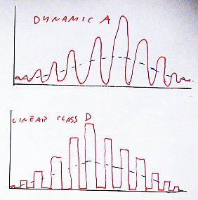 Now see
what happens in dynamic class A: The bias current starts as low as in
class AB, but is modulated so that the transistor never turns off. It
always gets just enough bias to remain in class A at any signal
amplitude, but just barely. At maximum amplitude the amplifier operates
exactly like a class A one.
Now see
what happens in dynamic class A: The bias current starts as low as in
class AB, but is modulated so that the transistor never turns off. It
always gets just enough bias to remain in class A at any signal
amplitude, but just barely. At maximum amplitude the amplifier operates
exactly like a class A one.
And the linear class D amplifier is pretty much the same thing, only
that a square wave is used for driving. This improves efficiency, but
only somewhat, because real world transistors do not switch fast enough
to actually produce clean square waves at radio frequencies. Using
class linear class D is an attempt at recovering some of the efficiency
lost when being forced to move from class AB to an operating class that
provides constant supply current over the RF cycle.
Some amplifiers operate with a sine drive at low drive levels, and the
drive squares up as they approach full drive. This is easy to implement
in BJT drivers, easier in any case than true squarewave driving. Such
amplifiers are often called class AB-D amplifiers, or class BD
amplifiers.
While I drew my crackly curves for BJT base current, they are also
reasonably applicable to MOSFET gate voltage, with some changes: The
horizontal zero line of the graph represents the gate threshold voltage
of the MOSFET, instead of 0V, and in the case of class AB and B
amplifiers the drive voltage waveforms aren't clipped on the negative
side, but extend all the way to their normal rounded peaks, even if
that means driving the gates negative. Of course that's theory, and in
practice they get highly distorted.
Driving a transistor:
While the output side of BJTs and MOSFETs is similiar enough to treat
them together, there are fundamental differences between driving a BJT
and a MOSFET, so we always need to consider the particularities of
each.
A BJT is fundamentally a current-controlled device, while a MOSFET is
voltage-controlled. At frequencies low enough to keep parasitic effects
low, a BJT's base voltage varies very little with drive, while it takes
a relatively large base current. The base input impedance is a very low
current-dependent
resistance, in parallel with a relatively small capacitance. An RF
power MOSFET instead needs from about 1V to several volt of RF drive at
the gate, while presenting an essentially capacitive impedance. The
gate behaves like a relatively large capacitor, with a small resistance
in series.
As we increase the frequency, both for the BJT and the MOSFET the
impedance values change. At sufficiently high frequencies the
inductances of the gate or base terminal and the internal bonding wires
start playing an increasingly important role, eventually becoming more
important than the capacitance and the resistance. At such high
frequencies the input impedances of BJTs and MOSFETs are much more
similar than at low frequencies. For moderate to high frequencies it's
best to consult the datasheet to find out the input impedance of a
given
transistor. In many cases it's given as a Smith plot, in other cases as
a table of values for several frequencies.
Instead at low frequencies it's often good enough to consider a
MOSFET's gate to behave like a capacitor, whose value is the
gate-source capacitance plus the product of the gate-drain capacitance
× the voltage gain of the particular amplifier (Miller effect).
A BJT operating at low frequencies can often be considered to have
nearly zero
RF base voltage for practical purposes, or a very low input resistance,
along with a parallel capacitance that is often small enough to ignore. At RF the BJT
will require a base drive current that is directly proportional to
frequency, for a given RF collector current. Its current gain is equal
to
its transistion frequency divided by the operating frequency, down to
such a frequency where the result equals the specified value
for
hfe. The current gain at the operating frequency can be multiplied by
the emitter resistance, given by 0.026 divided by the emitter current,
to get the base input resistance. For example a small BJT,
having
an Ft of 500MHz, operating in class A at 30MHz, with a current
of
0.05A, would have an emitter resistance of 0.52Ω, a current gain of
16.67, and thus a base input resistance of 8.67Ω in parallel with its
base-emitter capacitance plus its Miller capacitance. Larger BJTs,
operating at higher current, have an input resistance of a fraction of
an ohm, which eventually becomes dominated by ohmic resistance of the
connections, and is then dominated by the connection inductances. Since
the
current varies, the input resistance varies too - which introduces a
factor of nonlinearity, making the BJT have a very nonlinear transconductance. The current gain, though, tends to be
reasonably constant over a few decades of collector current, making
BJTs relatively linear current-controlled devices.
Some
people insist that BJTs are voltage-controlled devices, with a pretty
clean exponential transfer function. This is true too, of course, but
in most practical work it's easier to see the BJT as a pretty linear
current-controlled device, requiring a high drive current and a very
low, often negligible drive voltage.
It's important to understand that the calculated or datasheet-derived
input impedance of a BJT is only the average value over the RF cycle.
It varies dramatically over the cycle, due to the emitter
resistance and thus the base resistance varying with the instantaneous
emitter current. In any operating class other than A, the base-emitter
junction stops conducting over a part of the cycle,
causing dramatic impedance changes over the RF cycle.
When
driving the BJT from a resonant network, energy
storage (flywheel effect) in this network tends to absorb these
variations, but in low Q (broadband) situations the designer needs to
be very aware of this variation.
Driving a MOSFET at low frequency is mainly a matter of charging and
discharging its input capacitance. The drive current will then also be
roughly proportional to frequency, but is 90° out of phase with the
driving voltage. MOSFETs are highly non-linear voltage-controlled
current sources. The drain current varies fundamentally with the square
of the
gate voltage change, at least over the lower and mid drain current
range. Many amplifier circuits operate completely inside this very
non-linear range.
Both with MOSFETs and BJTs, the manufacturers usually add internal,
distributed source or emitter resistance. This serves to evenly
distribute the current over the entire chip, but also linearizes
the device by introducing negative feedback. Manufacturers select the
value of this internal resistance according to the intended
application of a transistor: Those intended for linear amplifiers get
larger resistance values, improving their linearity, while those
intended for nonlinear amplifiers get smaller resistors, which improves
the efficiency and gain. Transistors advertised for both linear and high
efficiency applications usually have an intermediate amount of
resistance built in.
The transfer curve of such a ballasted MOSFET starts with
the quadratic curve that's natural for all FETs, and gradually
straightens out
and then has a pretty linear high-current range. In a MOSFET
designed for
linear applications, the essentially linear range might start at about
20% of the maximum drain current. BJTs are reasonably linear
current-controlled current sources. When seen as voltage-controlled,
they become very non-linear, due to the exponential current-to-voltage
ratio of a semiconductor junction, but since the base-emitter
junction's
voltage variation is pretty small over the whole current
range, BJTs ballasted for
linear service are very linear from a very low collector current
onwards, maybe 2% of their maximum current, but they need significant
drive voltage, unlike non-ballasted BJTs. In any case, the fact that a
BJT's linear current gain
range starts at a much lower current than even a highly ballasted FET's
transconductance does, means that when operated in class
AB a BJT needs far less idling current than a MOSFET, for a given
degree of linearity. More about all this comes in the section about linearity.
All ballasting increases the saturation voltage, and thus has an impact
on efficiency. It also reduces the power gain of the device, due to the
degeneration it introduces. We can see it as built-in negative feedback.
The input circuit of an amplifier stage needs to perform at least two,
and often more actions:
- Biasing the transistors into the desired class, often
providing temperature compensation of the bias point.
- Matching the input impedance of the
transistors to the driving source, and in broadband amplifiers, often
provide gain
equalization over the frequency range.
- Reducing distortion, and further correcting frequency response,
through negative feedback.
The feedback circuit may also influence the bias, and usually it has an
important effect on input impedance. So the three functions are
intensely interrelated, which makes it hard to discuss them
separately. I will do my best, but there will be some mixing
of them.
Biasing:
RF power MOSFETs
are most commonly biased by applying an adjustable voltage to the
gates.
Depending on the power level involved, and the MOSFET's
characteristics, this voltage might need temperature compensation. The
gate does not draw any current from this bias source, so a simple
potentiometer connected to a regulated voltage source can be used. It's
important to properly design the bias circuit to have a suitable
internal impedance all the way from DC to the highest frequency at
which the MOSFET has any gain, and this impedance needs to be
considered in combination with drive and feedback circuits to either
hold the bias voltage constant through the RF cycle (class A, AB, C),
or to vary it in the proper way (mainly for dynamic class A).
In this biasing circuit a small 3-terminal regulator
provides bias voltage stabilization. Two diodes in series, thermally
coupled in the best possible way to the power MOSFET, provide thermal
compensation of the regulated voltage. These are slow diodes, so that
they aren't prone to rectifying any RF current picked up by their leads. A
bypass capacitor across them helps in this. The number of diodes can be
varied according to the characteristics of the MOSFET used. It needs to
be known that good temperature compensation can never be obtained, very
simply because the diodes don't accurately follow the temperature
changes of the MOSFETs die! Instead there is both a large attenuation,
and a very large time lag in their response. So it is always necessary
to design the amplifier in such a way that the MOSFET cannot go into a
thermal run-away situation faster than the sensing diodes can react and
reduce the bias voltage.
The regulated, roughly thermally
compensated voltage is applied to an adjustable voltage divider, that
allows setting the desired idling current for the MOSFET. Manufacturing
tolerances of the MOSFETs always require the bias voltage to be
adjustable. Since the regulated voltage is roughly 6.2V at room
temperature, going down at a rate of 4mV/K due to the two diodes, with
the divider values shown we can adjust the bias between about 2V and
6.2V at room temperature, with the thermal compensation varying along
with the adjusted voltage. In any practical application, the bias
circuit should be tailored so that the potentiometer allows adjusting
the MOSFET from fully off (gate voltage below the worst-case gate
threshold) to the highest voltage that could be required to set the
desired idling current in a particularly high-threshold, low
transconductance sample of the selected MOSFET type. This requires a
careful look at the MOSFET's datasheet. It is not desirable to make a
bias circuit with a much wider adjustment range than necessary, because
then it becomes more touchy to set the bias correctly.
Note
that the voltage divider in this circuit is configured in a safe way,
that is, if the potentiometer fails with its cursor contact opening
(a very common failure!), the bias voltage goes down, not up,
usually preventing the destruction of the MOSFET.
For further
amplifier design, in the areas of driving and feedback, it's essential
to understand what the impedance of the bias source is. In this
example, over the whole RF range the 1µF capacitor is a good bypass,
having negligible impedance, so that the bias source
impedance is
essentially just a 220Ω resistance. At DC instead this capacitor is an
open circuit, and the bias source impedance is the 220Ω in series with
the parallel combination of 470Ω and whatever value the potentiometer
is adjusted to. So the DC bias source impedance varies between 220 and
790Ω, according to the setting of the potentiometer. And in the
transition range between extremely low frequencies and RF, the bypass
capacitor has a reactance comparable to the resistances of the circuit,
and so the bias source impedance becomes complex. For example at 600Hz,
with the potentiometer set midway, the voltage divider has a source
resistance of 242Ω, and the capacitor has a reactance of -j265Ω . These
two appear in parallel, and that combination is in series with the 220Ω
resistor. The resulting bias source impedance is then 352-j121Ω, which
is the same as saying 372Ω with a phase angle of -19°. This phase angle
needs to be kept in sight, because it will causes a phase shift between
currents and voltages at the gate, which detracts from stability. More
about this will come further down, in the sections about feedback and
stability.
The bias circuit above is just an example. There are
many ways to do essentially the same job: Provide a regulated,
temperature-compensated, adjustable voltage, with a source
impedance that is known from DC to the highest frequencies at which the
transistor has any gain, and which is acceptable for designing the rest
of the amplifier.
In push-pull amplifiers it is often an advantage to have separate bias
voltage adjustment for each MOSFET. But if very well matched MOSFETs
are used, this isn't necessary.
Sometimes active bias stabilization is used, mostly with class
A amplifiers. Some sort of current sensor is used in the
supply
line, or in series with the source,
which could be as simple as a low value resistor with a small BJT
connected across it, and this is connected to the bias supply in such a
way that the operating current is stabilized at a constant value. This
eliminates the need for bias adjustment, and also for temperature
compensation, at the cost of some more components. The circuit needs to
be well designed to avoid instability. It's not very common in
practice.
MOSFETs typically require some
positive bias voltage even to operate in class C, in order to
keep
the conduction
cycle long enough for acceptable power output, and in some cases also
to avoid damage due to excessive negative gate voltage peaks. The
latter is
true particularly for LDMOSFETs, which typically tolerate far less
negative than positive gate voltage. So the bias circuit for MOSFETs in
class C is no different from that used in linear classes,
except
that
it must be possible to set the bias voltage low enough under the
MOSFET's conduction threshold to obtain the desired conduction angle.
Most commonly such bias circuits are configured to allow adjusting the
bias voltage between zero and about the highest expected gate threshold
voltage.
Power BJTs
used in linear service need a bias supply that can
be regulated from about 0.5 to
0.8V, and that can deliver a high current. The current required, with
some drive schemes, is as high as the maximum collector current divided
by the RF current gain of the BJT (transition frequency divided by
highest operating frequency). The bias voltage should remain very
stable even while the bias current varies over its full range.
This means that the bias source impedance must be extremely low,
preventing the use of a resistor to inject the bias into the
base.
Instead an RF choke is required, making the bias source inductive over
an extensive frequency range, which often causes stability trouble, mostly at very low frequencies.
The
bias voltage absolutely must be compensated for temperature, to avoid
thermal
run-away of BJTs.
Many circuits have been used, and they are widely published.
Designers in the 1970s loved to use the LM723. This IC
contains a
voltage reference, an operational amplifier, and a medium-current
driver transistor, allowing to easily wrap around a current sensing
diode, a potentiometer, a power transistor, and a few other parts like
bypass capacitors. Of course it's also possible to build a purely
discrete circuit, and this could be relatively simple:
The
two diodes cause a voltage drop of roughly 1.4V, which varies according
to diode temperature, and also according to the current passing through
the diodes, which is adjustable. The bias transistor drops this by
about 0.7V, depending on its own temperature, and the highly variable
bias current drawn by the RF transistor. In a perfect world, we would
thermally couple one diode to the RF transistor, and the other to the
bias transistor, to get optimal temperature compensation, but in
practice perfect thermal coupling is impossible, and so the usual
approach is to thermally couple both diodes to the RF transistor, and
mount the bias transistor on the same heatsink.
The
10Ω resistor has more than one function. One is providing a certain
minimum load to the bias source. This is necessary because when the
amplifier is idling, the RF BJT needs only a very small base current.
At this small current the base-emitter drop of the bias transistor
would drop significantly, producing significantly higher bias voltage.
The result is that the bias voltage would be poorly regulated, making
the amplifier run at excessive idling current. To fulfill this role,
the resistor can be located either where I drew it, or in parallel with
the 1000µF capacitor. But for stabiliy reasons its better to place it
where I drew it. Otherwise the undamped inductance of the choke might
lead to oscillation.
Another role of this resistor has to
do with the impedance of the driving source, and operating class. If
the driving source has a high output impedance, such as a transistor
operating without much shunt feedback, it acts as a current source.
Without the resistor at the base, it would combine with the rectifying
action of the base-emitter junction, and the RF choke's effect of
forcing a constant current over the entire RF period, to make the
amplifier operate in dynamic class A! This does not happen if the
driving source has a low impedance. A suitable resistor allows
operating in class AB even when the driving source has a high
impedance, and has no effect on this if the driver has a low impedance.
Seen in a very simplistic way, it does that by lowering the otherwise
high source impedance of a current-sourcing driver.
In addition, of course, the resistor has a swamping effect for the input impedance of the transistor.
The
RF choke in such a
circuit is a design problem. Its inductance needs to be low
enough
to be negligible at modulation frequencies, but high enough at RF. This
inductance causes serious current/voltage phase
shift, so that this choke is very often a big part of the problem when
such an amplifer self-oscillates. Often the choke is de-Q-ed by using a
very lossy core material, or by adding a resistor in parallel to the
choke, which RF-wise has the same effect as the base-to-ground
resistor, but does not consume additional current from the power
supply. The inductance value of a bias choke typically needs to be
pretty low, given the very low base impedance of RF power BJTs. This
low inductance might resonate with the transistor's input capacitance,
driver capacitance, and stray capacitances, well inside the operating
frequency range, causing a high risk of instability. The important
thing here is to always stay aware of the total
impedance to ground that a signal on the base sees, over a very wide
frequency range. The bias circuit is
involved, the drive circuit too, also the feedback circuit if present,
of course the RF transistor, and the base-to-ground resistor often
saves the day by both lowering this impedance and pulling its phase
angle closer to zero.
The large electrolytic capacitor provides
a low source impedance down to low modulation frequencies. This is
important because the bias transistor, operating as emitter follower,
has a low source impedance only while actually delivering current.
During operation of an amplifier, with its many parasitics and complex
modulation, there could be moments in which the choke current gets very
low, driving this transistor's emitter resistance way up, and the
amplifier might enter self-oscillation at a low frequency if that
electrolytic capacitor wasn't present. It's very often not possible to
make the value of the base-to-ground resistor low enough to stabilize
the amplifier in the absence of a big bias bypass capacitor, because
the amplifier would end up having no gain!
In low voltage BJT
amplifiers in the power range of about 1 to 20W it's somewhat common to
use a further simplified bias circuit:
The
disadvantage is that it constantly consumes a rather high current in
the bias diode, relative to the amplifier's power, and also that
adjustment of the bias level isn't very easy, because it would need
a potentiometer with a somewhat highish power dissipation
capability. So this circuit is mainly used with highly ballasted
transistors, which are a little less critical in their bias regulation
requirement. An experimenter can set the proper bias current
experimentally by chosing a suitable diode. Larger diodes have
a slightly lower voltage drop, at a given current. A transistor connected as superdiode is an option. In any case
the
current put through the diode must be higher than the
maximal average base current needed by the transistor at maximum drive. Very often this results
in a resistor lower than 100Ω, and capable of dissipating several watt.
It's a simple circuit, but not really good.
When I was a young ham, still a
student, and went backpacking with homebuilt radio gear and
nickel-cadmium batteries, having an efficient radio was crucial. But it
also had to be cheap! So I came up with the idea of using the current
standing in the class A driver to bias my class AB final stage. The
circuit ended up like this, seen in a cutout of the full schematic:
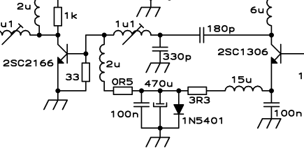
Never
mind that signals flow right-to-left in this circuit. Back in those
years I was fully omnidextrous... Anyway the emitter current of the
2SC1306 driver was put through the diode, instead of having to feed the
diode from the 12V supply via a lossy power resistor. The 3.3Ω resistor is part of the
driver's class A bias scheme - more about that later. The 0.5Ω resistor
causes a sloping bias curve, which sacrificed a little linearity in
exchange for higher efficiency, by moving the power amplifier's
operating point from AB to B and even slightly into class C on
modulation peaks. An added benefit of this trick is that turning on and
off the driver stage will automatically turn on and off the power
stage, which is great for very simple TX/RX switching. The driver's
current was enough to bias the power amplifier in this radio mainly
because the radio ran at just 7-7.3MHz, but used an RF transistor
having an Ft of about 100MHz, so the RF current gain was
relatively high and the base bias current required correspondingly low.
If you want to see this radio in full, it's here.
BJTs
can be very conveniently biased into class C operation by
grounding the base for DC. If this is done with an RF choke, it
typically needs to be de-Q-ed to prevent instability. Often the choke
is just a single ferrite bead, made of a very lossy ferrite type, or
else a low value resistor is placed in parallel with the RF choke.
It is very important to correctly decide how to inject the bias voltage
into a BJT amplifier, in combination with the driving circuit.
If
it is done in such a way that the bias current can freely vary, or that
the drive circuit can contribute current between the base and ground,
class AB operation can be obtained. If instead the bias voltage is
injected through an RF choke (or two), and the drive circuit isn't
ground-referenced (differential drive in push-pull stages), linear
class D or dynamic class A operation results. If an RF choke is used,
resistors from base
to ground can moderate this, and put the amplifier into hybrid
operation between class AB and class D, or even so close to class AB
that the remaining dynamic class A effects are absorbed in the idling
current band.
Consider the following three circuits of push-pull amplifier biasing
circuits, which differ only in the bias injection method:
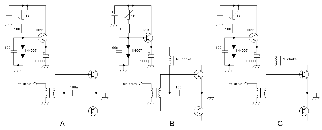
In
circuit A the center tap of the drive transformer is firmly held at a
fixed voltage of about 0.7V, by the combination of a local RF bypass
capacitor, a large electrolytic capacitor, and the bias voltage
regulating circuit. No matter what the drive signal does, the center
tap of the transformer will stay put at 0.7V (let's disregard for now
any small base-emitter drop changes with current). As a result of this,
and
assuming that the drive transformer has excellent coupling between the
two sides of its secondary, the voltage on the bases of the
two
power transistors will always vary in a symmetric way. If one base
voltage goes up a little bit, the other base voltage will go down by
the exact same amount. The current drawn by the bases is free to vary.
The instantaneous current put into the base of the transistor that is
conducting at a given time will depend on the drive current and the
transformation ratio, and it will ultimately come from the bias
regulator, flow through one half of the secondary, and on into the
transistor's base, with bypassing/smoothing provided by the capacitors,
so that the TIP31 doesn't need to vary its current at the RF rate (it
cannot, since it's too slow!). The other RF transistor's base will
conduct no current at all, because it's geting less voltage than
its conduction threshold, and so that side of the transformer
secondary will carry no current. Of course in the next half cycle
this reverses.
This
circuit allows to cleanly operate the amplifier in class AB, or class
B, or even class A if you want, just by properly setting the
potentiometer, and perhaps picking different diodes if necessary.
In
circuit B an RF choke has been added. This choke forces a constant
current in it over the RF cycle, but allows current changes at the
modulation rate. And the bypass capacitor at the transformer's center
point defeats the RF-rate current regulation provided by that RF choke,
so that circuit B really operates just like circuit A! The RF choke is
fundamentally superfluous, and the only reason why some designer might
want to use one is if the bias regulator is too far away from the
amplifier block, so that there is significant ground RF potential
difference between them. Anyway this is an unclean circuit, because any
reactance that the RF choke might still have at the modulation
frequencies will cause the bias voltage at the power transistors to
vary with modulation, and that will cause distortion. Circuit A works
cleaner, and is also less problematic in terms of stability.
Circuit
C operates in a totally different way: Since there is no bypass
capacitor at the drive transformer's center point, the constant current
forced by the RF choke over the RF cycle also forces the sum of the two
base currents to stay constant over the entire RF cycle! The total base
current can only vary at the modulation rate, but not at RF rate. So
the total collector current will do the same. The drive signal will
only act to distribute the total base current between the two
transistors, but cannot vary it inside the RF cycle! The result is
that this bias circuit cannot produce class AB, B, nor class C
operation. It can only be used for class A, including dynamic class A,
and for current-switching class D, including linear class D. Whether it
operates in class A or class D depends just on the
drive
signal: A sine wave for dynamic class A, and a square wave for class D.
Now
I get to one of the biggest pitfalls in linear push pull amplifier
input circuit design. It's the exact same that is common at the output
side: Poor or non-existing coupling between the two halves of the
transformer's winding!
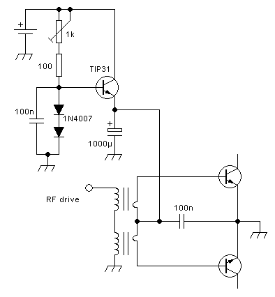
This
circuit shows such an input transformer that has no coupling between
the sides. It's what you get when you take a twin-hole ferrite core,
and wind a single turn for the low impedance winding. The two magnetic
circuits do not couple, and act like two separate transformers. Exactly
the same as in output transformers, described roughly five kilometers
up this page. An inexperienced designer will very likely think
that his amplifier using a single-turn, center-tapped secondary winding
drive transformer will behave like circuit A above, but no,
it behaves like circuit C instead! The designer intended to make a
class AB amplifier, and instead he gets a dynamic class A amplifier.
Instead of the expected 65 to 70% efficiency he gets only 40 to 45%!
The
same happens, of course, if he uses differential drive, without any
center tap, and injects the bias through separate chokes:
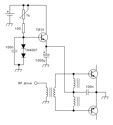
It's
just like with the output side of an amplifier: No cross-coupling
between sides, cannot work in class AB. The total base current cannot
vary over the RF cycle, allowing only class A or class D service.
Just
like in the single-ended amplifier, adding resistors from each base to
ground reduces the problem, and makes the amplifier operate in an
intermediate mode, much like class AB at low drive levels, and more
like dynamic class A at higher drive. Many amplifiers exist
that
operate in this way. They work, but they never have great performance.
Anyway BJT are obsolete for power RF use, so let's return to MOSFETs, and see how
to bias them for dynamic
class A!
You may think that it's crazy to do so, given that class AB
has
better performance than dynamic class A, and MOSFETs lend themselves
very easily for clean class AB biasing! The problem is on the output
side: As described about five and a quarter kilometers up in this web
page, it is extremely hard to achieve good cross-coupling between
drains in high power, low voltage amplifiers operating in the range of
100W to kilowatts. Hard enough to be practically impossible, if
operation up to the end of the HF range, and even beyond into low VHF,
is required. This can force a designer to intentionally run his circuit
in dynamic class A, and just accept the lower efficiency obtained, or
he might square up the drive signal and run the amplifier in
class D. To do so, the basic MOSFET biasing circuit needs to be adapted
in some way, to modulate the bias voltage according to the drive
signal's amplitude.
This can be done by common-mode feedback,
which I will describe in the section about feedback, or it can be done
by rectifying some of the drive signal. BJTs do the latter by
themselves, in their base-emitter junction, automatically producing
dynamic class A bias if allowed to do so. MOSFETs don't rectify
anything at their gates, so the rectifiers have to be added externally.
This can be done by injecting the bias voltage through diodes, like
this:
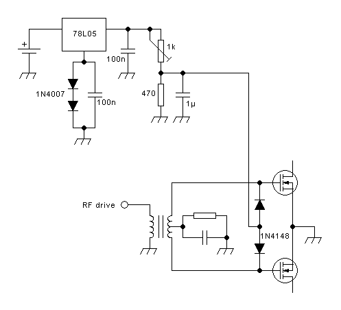
In
this circuit the gate voltage cannot ever go lower than the
voltage at the divider minus the diode drop. So, while there is no
drive signal, that's the voltage that will appear. But when there is
any drive signal, that's the voltage that will be on each gate during
the negative peaks of the drive signal, which means that the actual
bias voltage will get a modulation equal to half the peak-to-peak value of the drive
signal. The RC pair at the drive transformer's center tap has a cutoff
frequency that's much lower than the lowest RF frequency to be
amplified, but much higher than the highest modulating frequency. So
the centerpoint voltage, which is the effective bias voltage, follows
the modulation envelope, but does not follow the RF
signal, producing dynamic class A biasing.
Note
that since the center tap only needs to conduct low frequencies in this
circuit, this works well even if a twin-hole core with a single turn is
used.
But we don't even need a center tap! We can equally well
place an RC pair directly at each gate. And we don't even need to
physically add the capacitor, because the MOSFET gates are very
capacitive to start with! So the circuit morphs into this:
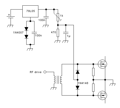
The
gate to ground resistors need to be dimensioned to give a suitable
cut-off frequency with the MOSFETs input capacitance, so they are
totally dependent on the MOSFETs used, and both the RF and
modulation frequencies. These resistors also have to be included in the
calculation of the bias voltage divider. The diode drops too, of
course.
In a practical circuit usually some more
resistors are added in various places, to tailor the bias modulation to
the optimal compromise between distortion, efficiency, drain
overvoltages, and so on. Various capacitors, chokes, beads, etc, might
need to be added for stability reasons. If separate bias control for
each MOSFET is desired, then one can add capacitors in series with the
transformer secondary, to break to DC path, and then feed each diode
from a separate voltage divider. And the bias voltage source could of
course be totally different from the one I'm showing in this chapter.
Since the gate to ground resistors might be relatively low, a bias
voltage source with a higher current capability is often required.
There are many possibilities, and since this is more a matter of power
supply design than RF amplifiers, I will control my urges and force
myself to abstain from presenting you two dozen circuit ideas for
this...
People casually looking at such bias circuits
with diode injection usually don't understand how this works, and why
the diodes are present. They just miss too many details to understand
the circuit: They don't "see" the capacitance of the gates, they don't
know about dynamic class A, and so on. So they often think that the
designer's intention, when he added those diodes, was to protect the
second MOSFET when the first one fails with a drain-gate blow-through.
But this is totally wrong! Designers usually don't care whether or not
in the event of a MOSFET failure the other one will fail too, because
anyway both will need to be replaced, both for the sake of matching and
because the still "good" one has very likely been degraded by the event
that killed its companion. The diodes are definitely there to implement
a dynamic, modulated bias, not for protection!
Let me warn you
that when studying published circuits you may also come across some
totally wrongly designed ones. It's very common that someone tries to
copy some design he doesn't fully understand, and makes "small" changes
which actually end up defeating the very purpose of the circuit he is
copying!
To round up the section about biasing, I will
quickly mention the biasing of small driver stages. While in higher
power class AB and dynamic class A stages it's pretty universal to have
potentiometers to set the optimal bias, it would be cumbersome and
unnecessary to have bias adjustments for every small stage.
But
some bias schemes used in small-signal amplifiers don't lend themselves
optimally for the typical pre-drivers, which are no longer really
small-signal, but are not really power stages either. I mean stages
running at an output power level of about 10mW to 1W, which are usually
operated in class A.
With BJTs it's very common to use just three resistors to bias them for
class A, in a pretty stable and reproducible way:
R1
and R2 form a voltage divider, setting the base of the transistor at
some convenient voltage, typically something between 1 and 4V. Then its
emitter is about 0.7V lower, giving a pretty well defined voltage
across R3, so that the value of R3 determines the idling
current
in the transistor. The absolute values of R1 and R2 are selected so
that a much larger current flows in them, than the expected base
current will be. This allows getting a pretty reproducible base voltage
regardless of the exact current gain of the actual transistor, and
that's important because the current gain of BJTs has a very wide
tolerance.
The higher a base voltage is chosen, the more stable
will the idling current be when the transistor changes temperature,
because the thermal change of its base-emitter drop will be less
significant relative to the voltage on R3. But a higher base voltage
also means that the maximum possible collector voltage swing gets
smaller, reducing the amplifier's maximum power output and efficiency.
So this is a tradeoff that the designer must make according to his
goals.
In practical circuits part or all of R3 is
often used to create negative feedback through emitter degeneration.
Part or all of R1 is also often used to create negative feedback, by
connecting the upper end of R1 to the collector instead of the supply.
More about this will come in the chapter about feedback.
This
same circuit can in principle also be used with small MOSFETs, but this
is less often done, because the gate-source voltage required for linear
operation of a MOSFET is several times larger, and also far less
predictable, than the base-emitter voltage of a BJT. So it would be
necessary to use roughly 6 to 10V or so at the MOSFET gate, and this
makes the approach unsuitable for typical low voltage circuits,
typically operating from something between 5 and 15V. But it's a
perfectly good method to use when running small MOSFET drivers from 30V
or more.
Small MOSFETs running from low voltage can still
use this circuit, if a MOSFET with very low and pretty stable gate
threshold voltage is used. In other cases small MOSFETs might need a
potentiometer for bias setting, just like their big brothers, or an
active biasing circuit. Since this is a chore, and anyway small BJTs
have far better linearity than small MOSFETs, and are still plentiful
and inexpensive, almost everybody uses BJTs in such small predriver
stages - or choses the lazy option of using IC RF amplifiers,
instead of designing his own discrete circuit!
Input impedance matching:
The same methods and circuits that are used for output impedance
matching can be applied to the input. That is, single-band amplifiers
can use tuned networks like the L network, the LCC to increase the Q,
or a series of several L networks to implement the
required matching with a lower
Q. The same equations given for output matching networks are used, but
since the transistor's input impedance is usually lower than the
driver's output
impedance, the networks are turned over: The parallel element of an L
matching network is placed on the input side. In VHF
and higher amplifiers,
the inductances are often implemented as microstriplines.
As an example let's consider a monoband 52MHz amplifier using a
MOSFET that under the expected operating conditions has an input
impedance of 0.8-j1.2Ω, glimpsed from the datasheet. This value means
that it behaves like a 0.8Ω resistor in series with a 2.55nF capacitor.
And the driver for this stage needs to be loaded with 13Ω,
free from any reactance. So we need a matching circuit that
transforms 0.8Ω into 13Ω at 52MHz, while also absorbing the capacitive
reactance of the gate.
Any online L network calculator can
quickly spit out that to match 13 to 0.8Ω at 52MHz, a capacitor of
919pF and an inductor of 9.6nH is required. But the series
equivalent capacitive reactance at the gate needs to add an equal
inductive reactance to the inductor, which brings its value up
to 13.2nH. The online calculator can spit out that change too,
or
it can be calculated the old-fashioned way, with a pocket calculator or
even a slide rule, if you are old enough to know what that is.
The matching circuit and its surroundings then looks like this:
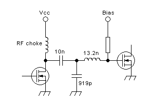
The
10nF capacitor is there just to block the DC. The 919pF
capacitor
would typically be either a trimmer of about 1200pF maximum
capacitance, or more likely a parallel combination of a smaller trimmer
and one or more fixed capacitors. The inductor could be implemented as
a microstripline (a glorified PCB track), which looks clean and is
cheap to make in mass production, or as very tiny coil having 1 or 2
turns of wire. The coil is easy to adjust by bending it, while the
stripline can only be adjusted by changing its dimensions, robbing us
of one adjustment point. On the other hand, changing the stripline's
length can be as simple as soldering the capacitors to it a little
closer or farther from the transistor.
The bias injection
resistor can double as a load resistor, to dampen down
unwanted
resonances and thus avoid instability. Of course the top side of that
resistor is bypassed to ground, etc... but here we are talking about the
matching circuit!
Broadband amplifiers can use conventional transformers or
transmission-line transformers. The conventional transformers are often
built using small two-hole cores with tube or braid secondaries, and a
few turns of wire as primary winding. For low power stages, twisted
wire pairs or trios wound on two-hole cores or even toroids are used.
As already mentioned in the biasing section, the same problems with
lack of side-to-side coupling in push-pull amplifiers that happen in
the output side also happen at the input, but since the input
transformers are physically smaller, these problems are somewhat easier
to avoid, and it's also quite possible to drive a push-pull amplifier
in differential mode, with no center tap at all on the transformer.
In most cases of broadband amplifiers it's necessary to compensate for
the capacitance in the transistor's input impedance. This is best done
by
absorbing the capacitance, and also the lead inductance, into a lowpass
section of sufficiently high cut-off frequency. In some cases,
specially when UHF transistors are used at HF, such compensation isn't
necessary, and instead the input capacitance is swamped by connecting a
low value resistor from the gate to ground, or better by providing
strong negative feedback. The resistor value, or equivalent load
resistance offered by the feedback circuit, in parallel with the
transistor's internal parallel-expressed resistance, needs to be
reasonably low compared to the reactance of the transistor's
parallel-expressed input capacitance, at the highest operating
frequency.
Let's
see examples of this, starting with the swamping technique. Assume that
you want to use a MOSFET that has an input capacitance of 100pF, in a
10W amplifier operating from 1.8 to 30MHz. The parallel equivalent
resistance in the input impedance will be high at the low end
of
the frequency range, so that the MOSFET itself needs almost no drive
power there, while at the high end of the range the parallel equivalent
resistance will be a lot lower. Since the input capacitance is roughly
constant, the reactance of this capacitance will also vary dramatically
over the frequency range. These variations are what makes gate swamping
so attractive! It allows a much more constant input impedance for which
to design, and it helps a lot in stabilizing the amplifier, although it
also wastes some drive power.
At 30MHz, the 100pF input
capacitance has a reactance of 53Ω. At 1.8MHz it will be 884Ω. The
resistive part of the input impedance tends to be reasonably close to
the reactive one, and it's very often not given in the datasheets for
all the frequencies we need, so we have to guess or measure, or just be
lazy: If we simply plant a 10Ω swamping resistor across the
gate
input, then over the whole range the total impedance won't change a
lot! If we assume the MOSFET to have roughly about the same input resistance
as it has reactance, at any frequency inside this range, then with our 10Ω
resistor added we might get a total 9.9Ω with a phase angle of roughly
-1° at 1.8MHz, while at 30MHz it will be around 8.3Ω at an angle of
-9°. This is close enough to consider the input impedance to be "essentially flat" in practice, over our whole frequency range!
But
this input impedance of roughly 9Ω average might not be the most
convenient. If we need the amplifier to be driven from a 50Ω source,
for example, it would be better to have a more convenient impedance
ratio than 5.5:1. So we can tweak our swamping resistor to
get
what we want: To use a simple 4:1 input transformer, we might use a
swamping resistor having about 14Ω. A more available value of 15Ω is
close enough, in practice. And we can use this resistor as bias
injection resistor too. And then our broadband matching circuit can end up
like this:
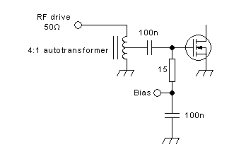
As you can see, it's nice and simple. The autotransformer used here can
very easily be wound with a few bifiliar turns of thin wire on a small
ferrite toroid or bead. The coupling and bypass capacitors
need to be large enough to have a low impedance relative to the roughly
13Ω load present, at the lowest operating frequency. The 100nF shown
here is about the minimum suitable value.
A circuit like this does have some droop in gain. At higher frequencies
the gate input impedance drops a lot, so that even while swamped by the
resistor it does have an effect. Also the gain of transistors, even
MOSFETs, drops with increasing frequency. In many applications the
droop is acceptable when it is as small as in this case, and
it is also possible to further reduce the droop by simply using a lower
value of swamping resistor, changing the transformer's ratio
accordingly to the new, lower, total input impedance, and accepting the
fact that now an even higher drive power is required. That means:
Brute-force gain flatness improvement costs gain!
There are some better ways to improve the gain flatness. These
become really important when a very wide frequency range is needed, or
when the MOSFET used does not have a very high maximum frequency. As
already indicated above, one such technique is to absorb the MOSFET's
input capacitance into a low pass filter, whose function isn't really
any filtering, but simply the seemingly magic disappearance of the
problematic high input capacitance of MOSFETs!
For example, let's assume that we want to extend the operating range of
our amplifier to 54MHz. Without compensation, and with a15Ω gate
swamping resistance, the gain of the stage would be down by a few dB at
54MHz, and the input SWR would begin to be on the poor side. So all we
have to do is design a π lowpass filter having a 13Ω impedance, a flat
passband, and using 100pF capacitors on each side. If we can
do that without this low pass filter cutting off any frequencies we
need, then we can use this method!
Low pass filters can be designed the hard way, by lots of manual
calculation, or the lazy way, by using software. Take your guess which
way I use... Plugging the values into the software, I come up with a low
pass filter using a 21.4nH inductor, that has a flat bandwidth of
107MHz, so it's plenty good enough! Its response looks like this:
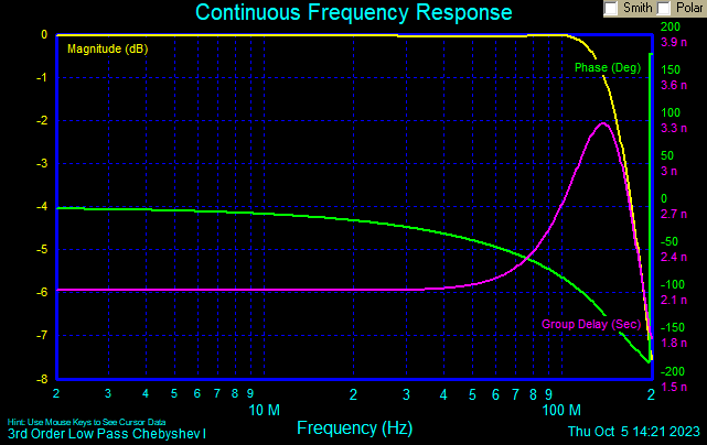
The magnitude response is essentially flat to well above the 54MHz we
need. The phase and delay aren't flat, of course, but these are
irrelevant as long as we don't include the filter in a feedback loop, and our signals are all narrow-banded.
So we can use this filter in our drive circuit:
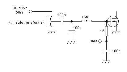
You surely spotted right away that I used a 15nH inductor, instead of
21.4nH. Why? Well, because the MOSFET has some lead inductance! We can
absorb that into the low pass filter's inductance, to make it disappear
too! The exact value of the inductor will depend on the PCB layout.
Often it's easiest to simply use a longish and narrow trace between
the MOSFET gate terminal and the 100pF capacitor, calculating it to get
the optimal inductance. Then the circuit on paper can be drawn as
having no inductor there, but just a capacitor from the gate to ground,
and people who don't understand this compensation technique wonder why
on earth the designer shunted the MOSFET's disturbing input
capacitance with even more capacitance... So, now you know
why there are so often capacitors connected directly between gate and
source, and often also drain and source! The trick is the transistor's
lead inductance! When working in the VHF range, very often even the
lead inductance is more than the compensating lowpass filter needs,
and so the leads need to be shortened, or the capacitors need to be
soldered extremely close to the transistor's body, right where the
leads come out.
The larger the lead inductance is, relative to the total lowpass
filter inductance, the less well is the swamping/loading resistor
placed. This worsens the performance of the circuit. That's why I drew
the resistor connected so close to the MOSFETs body! In the example
shown here, it still works pretty well, but in VHF and UHF circuits it
often makes little or no sense to use any swamping resistance. Anyway
at such frequencies the internal resistance of the MOSFETs input is
pretty low, and typically such amplifiers are tuned to a single band,
so things are all different. Absorbing the gate capacitance into a low
pass filter is a technique mostly useful for broadband amplifiers used
at
HF and into low VHF.
In high power BJT input circuits it was common to use frequency
response compensation with various arrangements of RC and RL
groups, to achieve acceptable gain flatness along with acceptable SWR
at the input. This was very necessary, because BJTs have a far more
drastic gain droop with frequency than MOSFETs do, and also
because in the age of BJTs we often built 1.8-30MHz amplifiers with
BJTs having an Ft of barely 100MHz. So the current gain of those
transistors was only about 3 at the highest frequency, but over 50 at
the lowest frequency! And with power gain being proportional to the
square of current gain, that made for a massive gain difference over
the frequency range.
A typical BJT frequency compensating drive circuit could have looked
like this:
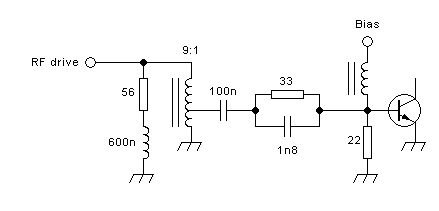
Please don't take the component values given in this schematic as a
golden recipe! They need to be optimized for each particular
application, depending on the transistor used, power level, frequency
range, desired input impedance, tradeoffs between gain flatness and
basic gain, and so on. In any case, the idea is that at high
frequencies the 600nH inductor has a high reactance, and the 1.8nF
capacitor has a low one, so that most of the drive power gets to the
transistor, and the autotransformer provides the proper match. At low
frequencies instead the 1.8nF capacitor has a high reactance, so there
is far less drive current, with most of it going through the 33Ω
resistor, the autotransformer sees a relatively high load impedance,
and the 600nH inductor has a low reactance, so that the 56Ω resistor
can load the drive source to keep the total input impedance of the
amplifier close to 50Ω. The 1.8nF capacitor also introduces a pretty
strong capacitive reactance into the circuit's input impedance, while
the 600nH inductor introduces a suitable inductive reactance, and if
all the component values are properly chosen to work optimally
together, then the input impedance will not stray too much from a
purely resistive 50Ω.
Such a circuit can be fully calculated, but it's a bit complex. It can
also be pre-optimized empirically in a circuit simulator, with the
final optimization being done in the good old style, with a soldering
iron and a good selection of parts to try. Since these days we rarely
use BJTs for RF power amplification, we can probably let this matter
rest. It's useful mainly to understand how old, existing equipment
works.
Small BJTs
are still often used in drivers and pre-drivers below the 1W level. So
it's important to understand how to drive these. The input capacitance
of such transistors is usually very small, and can be neglected in most
cases. But the BJT's input resistance varies dramatically over the
frequency range, because it depends on the transistor's current gain,
which in turn varies inversely with frequency. The input resistance is
the emitter resistance multiplied by the current gain. The emitter
resistance is roughly 0.026 divided by the collector current,
for silicon transistors, and the current gain is the transistor's Ft
divided by the operating frequency. So, if we are building a class A
predriver that will operate with an idling current of 30mA, its emitter
resistance is
0.026 ÷ 0.03A = 0.87Ω
This is the internal emitter resistance at this current. If the
amplifier has any additional external, non-bypassed resistance in
series with the transistor's emitter, then this resistance has to be
added to the internal one, for all further input resistance
calculations.
If we are running it at 30MHz at a given time, and the transistor has
an Ft of 500MHz, then its current gain is 16.7, and if there is no
external emitter resistor, its base input resistance ends up
being 14.5Ω. But at 1.8MHz the current gain may be as high as 278,
although it will more likely be clipped by the DC current gain (hfe),
to a value typically anywhere between 50 and 200. So the base input
resistance at 1.8MHz could be anything between about 43 and 170Ω.
Since the input resistance is so variable, we need to swamp it in some
way, to get a reasonably stable total resistance to which we can match.
This is often done by selecting low value bias resistors, but it's even
more common to do it with negative feedback. We will get to this soon!
Often it's a good idea to add a few ohm of external emitter resistance,
to drive the transistors input resistance to a value well above 50Ω.
Then we can swamp it with a 51 or 56Ω resistor, and get a direct match
to a 50Ω source, without any further effort. The cost of this is
getting lower gain, but there is also the benefit of better linearity.
The base input capacitance of such small BJTs is just a few pF, so the
capacitive reactance is very high compared to the resistance, and we
usually don't need to care about it. As a result, we can match the
input of our pre-driver stage to the signal source by any of the common
techniques, such as autotransformers, plain transformers,
transmission-line transformers, or tuned matching networks in the case
of
single-band amplifiers.
Here is a very simplistic and somewhat stupid little example of a
directly matched small amplifier's input circuit:
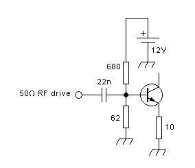
The bias voltage divider provides 1V at the base, assuming
that it isn't loaded by the base current. Assuming 30mA collector
current, and an hfe of 100, there are 0.3mA of base current. Relative
to the 16mA flowing in that voltage divider, 0.3mA is very
little, so we will indeed get very close to 1V at the base. Just a tad
less. The emitter will then be at pretty precisely 0.3V, and the 10Ω
resistor will indeed set the emitter current to 30mA. So we have done
the biasing part for 30mA.
Then comes the RF part: At 30mA we have 0.87Ω internal
emitter resistance. Plus the external 10Ω , it's 10.87Ω. Given that this transistor
has an Ft of 500MHz, at our highest
(worst case) frequency of 30MHz the current gain is 16.7, so the base input resistance
is 182Ω. The bias voltage divider has a source resistance of 57Ω. In
parallel with the 182Ω, that's 43.3Ω total input resistance. Close
enough to 50Ω for direct connection. And at 1.8MHz the transistor's
input resistance will be at least 550Ω or so, which in parallel with
the divider's resistance is just a little above 50Ω. Close enough for
direct connection too! So we don't need any further
impedance matching - if we wanted a 50Ω input impedance, of
course!
So here you got your first example of a circuit that shares
three resistors between biasing and impedance matching functions! Each
of those three resistors is used for each of the two
functions.
Note that in this circuit I changed the coupling capacitor to 22nF, for
no other reason than to remind you that coupling capacitors don't
always need to be 100nF! :-) 22nF has a reactance of just 4Ω
at 1.8MHz, which is still low enough for good coupling in
a 50Ω circuit.
Small MOSFETs
are very different animals in this regard. They have a high input
capacitance, with very little series resistance. So we basically need
to drive a capacitor. This could be 50pF or more, depending on the
MOSFET used. This usually cannot be neglected, particularly because
there is so little resistance present. So the usual practice with
broadband drivers is to swamp it with a resistor, or preferably
negative feedback, giving a total input impedance so low that the
capacitance remains a reasonably irrelevant part of it even at the
highest frequency of operation. But it is also possible to use the low
pass filter compensation technique, and this results in much greater
gain, since a lot less swamping is needed.
Since MOSFETs are also harder to bias to a stable operating
point, and are less linear than BJTs, my advice is to avoid them, and
stick to BJTs for small driver stages, as long as such BJTs remain
available.
When driving a push-pull
stage its important to understand what
combination of differential-mode and common-mode drive you are
implementing. I think it's again time for a Blue Block!
The split personality of
push-pull amplifiers
Single-transistor amplifier stages are straight and honest: What goes
in at their single drive input, comes out (hopefully amplified and
clean) from their single output. But push-pull amplifiers
aren't like that. Having two inputs and two outputs, at least
internally, they can do all sorts of mischief - and they love to do it!
What you put in at only one drive input might come out from only one
output, or only the other one, or both in phase, or both in
opposite phase, or not at all. What you put into both inputs in the
same phase offers the same range of options for where and how it will
come out, if at all. Only if you put the same signal into both inputs
but in phase opposition, do you have a pretty good chance that it will
come out the same way, that is, from both outputs and in phase
opposition. Of course it might come out larger from one output than the
other, which means that part of it is coming out as it should, while
another part is coming out from only one output... You get
the idea! You really need to watch them closely, or they will
catch you by surprise.
Consider the following, very simple, basic and stupid circuit:
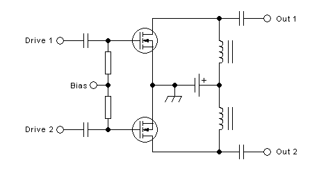
It's a
push-pull amplifier that's built basically as two completely
separate single-ended amplifiers, that only share the power and bias
supplies. As long as we don't interconnect the inputs and outputs in
specific ways, this amplifier is capable of being mischievous. Any
signal that you apply between the two inputs will come out at both
outputs in opposite phase, so that a load placed between the two
outputs will see it. But if you place the same signal at both inputs in
parallel (that's called a common-mode signal), it will also come out at
both inputs in the same phase, which means that a load connected
between the outputs won't see it. This is fine, since a good
push-pull amplifier is supposed to suppress common-mode signals - but
only until you realize that each of the two transistors will still see
all of the signal, will amplify it, but will see no load, because the
load gets the same signal at both terminals! So both transistors will put
out a full-amplitude, clipped, square wave voltage, even if the drive signal is
small and a sine wave! In practice this means that if you have such an
amplifier, with a load between its outputs, even the smallest
common-mode input signal applied together with the main differential
drive signal will make it saturate like crazy, and distort the main
signal! In other words, your drive signal needs to be perfectly
symmetric. And perfection doesn't exist in real-world electronics.
Fortunately there are usually so many imperfections present, that they
tend to make the circuit more tolerant. One imperfection gives way
where another is pushing. For example, the chokes used to feed the
drains will be lossy, which means that they act like if there were
resistors in parallel to each of them. These resistors form an
additional load on the amplifier's outputs, which is independent on
each side, and thus can absorb small common-mode output currents and
keep the amplifier from saturating on them.
The crucial thing to always keep in mind when working with push-pull
amplifiers is that they have two modes of operation: Differential mode
(the desired one), and common mode (the parasitic, usually undesired
one). You always need to analyze what happens in each of the two modes,
to reduce the number of surprises a push-pull amplifier gives you. If
you apply two drive signals in opposite phase, as is normal, the two
transistors will work in opposed phase, and a load placed between the
two outputs will get the output power. Instead if you apply a drive
signal in the same phase to each side, both transistors will work
happily in the same phase, the differentially connected load will get
nothing, but the transistors might actually kill themselves from the
inductively generated voltage spikes of the drain feed chokes, which
have nowhere to go except straight through the transistors! End even if
you apply perfectly differential drive, but the inevitable
imperfections in the amplifier turn part of that into a common-mode
signal, you can get those damaging common-mode voltages!
Differential and common mode applies not just to drive and output
signals, but also to feedback, and to self-oscillation. Even if a
push-pull amplifer is driven in a perfectly balanced way, amplifying in
the desired differential mode, and loaded in a balanced way, it might
self-oscillate in common mode, because the designer forgot to make sure
that the common-mode stability is adequate.
Center-tapped push-pull transformers, or balanced (bifiliar) feed or
bias chokes, couple the two sides together in opposite phase,
preventing significant common-mode voltages from appearing - at least
as long as these transformers actually work as intended, which is often
not the case...! But designers often forget that electronics is not
just a world of voltages, but it's just as much a world of currents! When
you suppress common-mode voltages by using such means, usually you are
giving totally unrestricted way to common-mode currents! So
even if you have excellent side-to-side cross-coupling in a push pull
amplifier, you still need to do the common-mode stability analysis, and
it's good to learn to "see" voltages and
currents in both the differential and common modes.
Feedback:
Negative feedback is a very powerful tool to reduce all kinds of
distortion, stabilize the bias and the gain, flatten the frequency
response,
and make an amplifier's performance largely independent from the
specific transistor's characteristics. Some amateur designers are
frightened by it and try to avoid it, but in fact all amplifiers have
some unavoidable negative feedback! If it's not explicitly implemented
in the circuit, it will happen through the transistor's internal
output-input capacitance, and through degeneration from internal and
external inductance and resistance in the emitter or source connection.
Undesired capacitive and inductive feedback in the external circuit is
also always present to some extent. Most of these natural negative
feedback paths are highly reactive, and thus facilitate
self-oscillation, by shifting the phase in a frequency-dependent manner. Intentionally applied feedback instead can be made
mostly resistive, and can be made strong enough to swamp the undesired
reactive feedback, stabilizing an amplifier that would oscillate
without it.
Negative feedback always costs gain. For that reason typically it's not
intentionally used in single-band amplifiers operating at a frequency
that's close to the highest one the selected transistor is good for,
because at such frequencies only little gain is available, and we want
it all. But small transistors often have a huge power gain at HF, and
LDMOSFETs have a huge power gain at HF even while being high power
devices. So we can very well consume some of this gain in negative
feedback, to improve the linearity, stability and gain flatness
of a broadband linear amplifier.
Transistors
are highly nonlinear devices, with MOSFETs being worse than BJTs. If we
want to build linear amplifiers using them, correctly applied
negative
feedback is a crucial tool to achieve this goal. Amateur designers
who avoid it, because they don't understand it, can never
achieve
the performance of a correctly designed amplifier that uses negative
feedback to advantage.
In push-pull stages we need to design the feedback to work in
differential and/or common mode, depending on what we want to achive.
And in any amplifier we need to make sure that the feedback stays
negative over the entire frequency range in which the amplifier has any
gain, even far outside our actual operating frequency range, or we will
end up with an oscillator instead of an amplifier.
The
principle of negative feedback should be known to anyone reading this
article, but if you still have a gaping hole in this area of your
knowledge, I can quickly fill it in. Negative feedback is very easy to
understand, and works in a highly perfect way in operational
amplifiers:
The operational amplifier compares the
voltage between its two inputs, and amplifiers the difference between
them by a very high factor. The two resistors act as a voltage divider
between the input and output, and so the operational amplifier will
generate whatever output voltage is required to make that voltage
divider deliver the exact same voltage to the negative input, as the
positive one is getting from the reference voltage source. The output
voltage is then the difference between the input voltage and the
reference voltage, multiplied by the ratio between R2 and R1. It does
not depend significantly on the actual gain of the operational
amplifier, and this means that if its gain varies due to frequency,
temperature, tolerances, or even if it varies dynamically with voltage
level (that is, the operational amplifier causes distortion), the
output voltage will still be a very clean, predictable multiple of the
difference between the reference and the input voltage, defined by the
two resistors. So, as long as the operational amplifier has enough
gain, it doesn't need to be good in terms of distortion nor gain
flatness, and the complete amplifier will still be excellent,
clean and predictable.
Transistors work the same way, only with
less gain than an operational amplifier. In exchange for that they can
work at much higher power levels, and to much higher frequencies.
The
reference in a BJT is the voltage at the emitter, incremented by the base-emitter diode
drop of about 0.7V. And since a transistor doesn't have additional pins
to connect the power supply, we need to power it at its collector, done
here with resistor. Otherwise it's the same circuit as that using the operational amplifier.
And this circuit indeed works essentially in the same
way as the operational amplifier circuit: The voltage gain depends
mainly on the ratio between R2 and R1, and the output signal has very
little distortion, despite the transistor being a nonlinear
device. Also the gain of the amplifier stays essentially constant up to a pretty high
frequency, despite the transistor's gain being inversely proportional
to frequency over most of the range.
A MOSFET can be used
instead of a BJT, but it's less good: The MOSFET has much lower voltage
gain in a typical circuit, so the output voltage depends much more on
the transistor's characteristics than in case of a BJT amplifier. Also
the much higher input capacitance of a MOSFET can cause more limitation
of the usable frequency range. But the details depend on the actual
characteristics of each particular device. MOSFET technology keeps improving, and
each year MOSFETs are taking over some more application area from BJTs.
Negative
feedback, implemented in this way, not only reduces the gain, but also
reduces the input resistance at the base or gate. It acts just like a
swamping resistor in this regard, but while a wamping resistor to
ground simply wastes drive power in exchange for a more stable and
neutral input impedance, negative feedback wastes that same drive power
in exchange for that same more stable and neutral input impedance, plus lower
distortion, plus
a flatter frequency response! So it's a very much better deal, and
every good designer prefers using negative feedback instead of plain
resistive input swamping.
I had already mentioned
in the input matching chapter that any resistance in series with the
emitter of a transistor causes an increase of input
resistance.
Well, it also causes strong negative feedback, because whenever the
collector-emitter path conducts more current, this causes a higher
voltage drop on the emitter resistor, reducing the base-emitter voltage
and thus reducing the collector-emitter current. This kind of negative
feedback is present in every amplifier stage, due to the unavoidable
internal emitter or source resistance of transistors, and also due to
their lead inductance, which causes the same feedback effect but with
90° phase shifting. Transistor manufacturers intentionally add small
amounts of this resistance right inside, where it's associated with the
least inductance, when making medium power transistors. In low power
transistors the circuit designer can add it externally, and in high
current transistors this effect typically becomes larger than
desirable, reducing the gain too much, and it has to be reduced by
using several very wide emitter or source connections, or even by
manufacturing MOSFETs in a laterally diffused fashion with
through-the-chip source contacts, so that the entire underside of the
silicon chip becomes the source connection, and can be directly
soldered to the metal base of the transistor, the heatsink, and the
circuit, with extremely short and wide connections.
Let's
see what each form of negative feedback does to an amplifier. To begin,
I will start with a simple amplifier that has no intentional feedback:
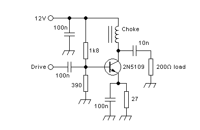
The
bias voltage divider would produce a tad over 2V at the base, if there
was no base current. This gives around 1.4V at the emitter. With the
27Ω emitter resistor, the transistor takes slightly over 50mA.
This in turn creates roughly 0.5mA base current, which loads the
divider, which has about 5mA flowing in it. So it gets slightly pulled
down, and the transistor will end up biased to slightly less than 50mA.
Its
internal emitter resistance is then 0.5Ω. For RF the emitter is
grounded via a capacitor, so the transistor's input resistance is
simply 0.5Ω multiplied by the RF current gain. The transistor has an Ft
of 1200MHz, so at 30MHz its gain is 40, and its input
resistance
is 20Ω, and this varies in inverse proportion to frequency, except
below about 15 or 20MHz, where the current gain gets capped by the
(highly part-dependent) hfe.
Let's take 30MHz as a frequency for
our calculations. 1mV of drive signal, appearing on the 0.5Ω emitter
resistance, create 2mA of collector current. This RF current cannot go
through the choke, so it all goes through the load resistance. Since
this is 200Ω, there will be 400mV at the output. So this amplifier has
a voltage gain of 400 at 30MHz.
Let's see it current-wise: A 1µA
drive signal will mostly go into the base, because the bias divider has
a pretty high resistance relative to the 20Ω base resistance of the
transistor. The transistor has a current gain of 40 at 30MHz,
so
the collector current is 40µA. All of this can only flow through the
load, and so the current gain of this amplifier is 40.
That's a
10:1 ratio between voltage gain and current gain, which makes total
sense when you consider that the input resistance is 20Ω and the output
resistance is 200Ω.
Many designers like to talk about gain in
terms of dB. But dB is a power ratio, not a voltage or current ratio.
When input and output resistances are different, one needs to be
careful about this! Taking the standard equation to express voltage
gain in dB, a gain of 400 is 52dB, but the current gain of 40 is only
32dB. When driving the amplifier with 1mV, the 20Ω input resistance
allows 50µA to flow, and that's 50nW drive power. At the same time the
output is 400mV, 2mA, and that's 800µW. That's a power gain of 16000,
and that equates to a power gain of 42dB, which is the final word on
the matter.
Remember that the gain in dB is 10×log(Pout÷Pin) .
Also remember that only when input and output impedances are identical,
the gain in dB is 20×log(Vout÷Vin), or 20×log(Iout÷Iin).
How
much output power can we get? The transistor can pull its collector
voltage down to a little under 2V, so the the possible swing is ±10V
around the 12V supply, and that's 7.1V RMS. The transistor is biased to
a little less than 50mA. 10V in 200Ω makes 50mA flow, so in
fact
we will run out of peak current a little bit before we run out of peak
voltage capability. Let's take 45mA as the clean peak load current.
That's 32mA RMS, and in 200Ω that's 200mW. The input power is given by
the 12V supply and the slightly less than 50mA collector current plus
5mA bias divider current, so it's about 620mW. So this amplifier has an
efficiency of around 32%, which is totally typical for practical small
class A power amplifiers.
Note that in the real world both the gain and the input impedance will
be lower, though, because this amplifier is not
free from collector-to-base feedback! The transistor used
has an
internal collector-base capacitance, there is also external capacitance
there, and this pushes the input impedance down, and also rotates its
phase, consumes some of the output current, and draws additional drive
current. The datasheet of the transistor doesn't give the value of this
capacitance, so we are on our own there. Also the frequency range over
which these calculations hold true will be restricted by parasitic
components, such as the inductance in series with the emitter lead and
the emitter bypass capacitor.
Anyway the gain of such
a feedback-less amplifier is very high, and this high gain usually
creates stability problems. Also the entire nonlinearity of the
transistor will affect the signal, and both the gain and the input
resistance will be strongly frequency-dependent above a certain cutoff
frequency, because the current gain of the transistor changes with
frequency. So we get an unstable, non-linear, very frequency-dependent,
high gain amplifier.
Let's improve that. Let's sacrifice some gain for improvements in the
other areas!
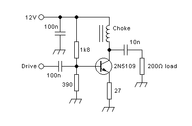
The
only difference in this circuit is that I removed the bypass capacitor at the emitter,
introducing strong negative feedback through emitter degeneration. The
DC biasing has not been changed. But the effective emitter
resistance is now the internal 0.5Ω plus the external 27Ω, a whopping
difference! At 30MHz, current gain 40, the input resistance of the
transistor is now 1100Ω! It gets swamped by the equivalent resistance
of the bias voltage divider, 320Ω, to make a total input resistance at
30MHz of 248Ω. That's a whole lot higher than it was before! It will
also change a lot less with frequency, due to the swamping.
1mV
of input drive , appearing on the 27.5Ω total emitter resistance, makes
36µA of collector signal current, and thus output current, which in
200Ω makes 7.27mV. That's a voltage gain of 7.27. It can also be calculated easier as
200÷27.5.
1µA of drive current will divide into 225nA into the
base, and the rest going into the bias resistors. At a transistor
current gain of 40, that makes 9mA output current. That's a current gain of 9.
And thus a power gain of 66, equating to 18dB. That's
certainly a
whole lot less gain than before, but it comes with a good gain flatness
over a wide frequency range, a much higher and more stable input
impedance, lower distortion, and better stability.
An
amplifier like this, even while designed for a load resistance of 200Ω,
has a very much higher internal output resistance. This means that it
behaves largely like a current source. It will tend to force a certain
current into the load, no matter what impedance that load has.
So this amplifier has no trouble if the output is shorted. It will just
put a controlled current into the short circuit, essentially the same
current it would put into the load resistance. But if the load
is
disconnected, it will try to put its current into the almost infinite impedance of the choke!
The negative peaks cannot go below a collector voltage of about 1.6V,
but there is no real limit set by the circuit for the positive peaks.
They can rise as high as required to... guess what? To
destroy
the transistor!!! So this amplifier cannot handle an open output.
Now let's trade emitter degeneration for shunt feedback:
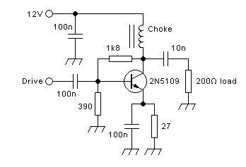
The
capacitor at the emitter is back, turning off almost all of the emitter
degeneration (the small amount caused by the transistor's internal
emitter resistance remains), and the upper bias resistor has been moved
to the collector. This change makes no difference in terms of DC
biasing, since the collector is at 12V DC potential, due to the choke
being incapable of causing a voltage drop at DC. But now the 1.8kΩ
resistor provides a path for RF negative feedback. Let's see what
happens:
At 1mV drive, the transistor puts 2mA signal current
through its collector, like in the feedback-less case. The total load
is now 200Ω in parallel with a little less than 1800Ω. A little less
because the base signal voltage is in opposite phase to the collector
voltage. Since here the voltage gain is so high, we can neglect this
difference and calculate simply with 1800Ω. So the effective load
resistance is 180Ω, and the output voltage is 360mV, the voltage gain
is 360, not much different from the feedback-less amplifier. But the
360mV make 200µA flow in the resistor, which loads the input, while the
transistor's base is only taking 50µA from the input! So the shunt
feedback
makes the input resistance of the amplifier much lower: At 1mV
drive voltage, we now have a total drive current of 250µA, so the input
resistance of the amplifier has dropped to just 4Ω!
So we have
sacrificed just a little voltage gain, but a considerable
amount
of current gain, in exchange for better linearity, stability, and
flatter frequency response.
The power gain is now 34dB. The fact
that we sacrificed less gain is not due to the type of feedback, but to
the amount of it. We can of course vary the amount of both types of
feedback, by adjusting the resistor values as required.
Note
what happens if we now disconnect the load: At a given drive voltage,
such as 1mV, the collector signal current will then all have to go
through the feedback resistor. With the resistor values used in this
example, the output voltage would then increase only 10-fold, which is
a huge improvement over the amplifier that has no feedback of this
sort. Making the shunt feedback a little stronger, we can make
this amplifier safe against load disconnections.
Since shunt feedback tends to stabilize the output voltage, no
matter how much
current the load demands, it makes the amplifier have a low internal
output resistance: It behaves more like a voltage source. So it may not
survive an output short! If the drive signal is strong enough, it might
make the amplifier self-destroy by trying to put more current
into
the shorted load than the transistor can handle.
So:
Shunt feedback protects against open loads, and
reduces
input and output resistances. Emitter degeneration instead
protects against output shorts, and increases input and output
resistances. Both of them reduce the gain, and improve linearity. Both
of them improve stability, as long as no parasitic effects come into
play. In this regard, emitter degeneration can be problematic: Too much
of it can degrade stability!
A nice thing in this is
that by properly balancing the amount of the two kinds of feedback, we
can make an amplifier have a certain desired input resistance, and keep
it quite stable over a wide frequency range, while also being
relatively tolerant of load impedance changes, have pretty stable gain
of our choice over a wide frequency range, have a low distortion, and be free from
any self-oscillations. We pay for all this in the maximum achievable gain. The gain
is
always lower when negative feedback is used. When our
transistor
has lots of gain that's not a problem at all, but when we need lots of
gain and the transistor doesn't have very much we might need to
increase the number of amplifier stages, to enable us to get an
amplifier with the required frequency response, gain flatness and low distortion.
For
this little amplifier I selected a nominal load resistance value of
200Ω, because it was a good fit for the12V supply and the 50mA
collector current value from which I arbitrarily started. But when the capability
to optimally drive a 50Ω load is desired, it's extremely easy
to
convert
this amplfiier to a 50Ω output: Just replace the choke by a 4:1
autotransformer! This is done by winding the exact same
amount of
wire, on the same core, but winding it as a bifiliar pair, with the
same number of total turns, that is half the number of
bifiliar
turns:
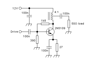
Note that I also increased the value of the
coupling capacitor, to account for the lower load resistance. I stuck
to the old custom of using round values of capacitance, although of
course in an actual design one would check this against the true
requirement according to the lowest required operating frequency.
The
power supply bypass capacitor becomes more important in this circuit
configuration, because it has to carry half of the output's RF current.
Ideally the ground terminal of that capacitor should be close to the
load's ground point.
With this modification amplifier works just
the same, with the same power gain, over the whole frequency range in
which the autotransformer has good coupling.
In principle any transformation ratio can be implemented in this way, but
4:1 is the easiest to do.
Now
let's consider a much-used,
practical, very low power amplifier stage, that has both forms of
negative
feedback:
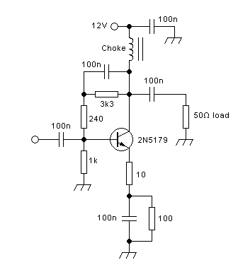
This
circuit has been published many times in US-American ham literature,
almost since the beginning of small RF transistors, with some variations.
I'm showing you this circuit to illustrate the use of RRC networks both
at the emitter and in the shunt feedback path, which allows separate
control over the shunt feedback, the emitter
degeneration, the input resistance, the bias current,
and the
base voltage. It's a good circuit for learning how to tailor such a
circuit for specific needs, and
that's why I'm mentioning it. Many hams have copied this circuit
without fully understanding it. Let's try to do better!
The
base bias voltage divider has 3540Ω total in the upper leg, and 1kΩ in
the lower. Connecting its upper side to the collector instead of
directly to 12V is of course just the same, for DC purposes, because
the choke can cause no significant voltage drop at DC. So in the
absence of any base current we would get a base voltage of 2.64V, giving
about 2V at the emitter. Since the total emitter resistance is 110Ω,
plus a small amount inside the transistor that can be ignored relative
to 110Ω, the emitter current is around 18mA. The typical hfe of the
transistor used is given as 70 in the datasheet, although it has a very
wide tolerance. Let's use 70 for the calculation: The base bias current
is then 0.26mA. That's about one tenth of the current standing in the
base bias divider, so it will pull the voltages and currents a little
down, and the transistor will finally end up conducting about 16mA.
We can't be ultra-accurate here, because anyway the hfe of a BJT has a
very wide tolerance. Bias business done!
With that current, the internal emitter
resistance is about 1.6Ω, and for RF purposes this is in series with
just the 10Ω of unbypassed external emitter resistance. So we have
11.6Ω total. The typical Ft of this transistor is given as 1.4GHz. So,
if properly assembled, with very small, low inductance parts,
ideally SMDs, it would be reasonable to expect this circuit to
work into the range of a few hundred MHz. At 300MHz the
current
gain would be 4.7, and the input resistance of the transistor 54Ω. At
lower frequencies both of them rise accordingly, down to about
20MHz, where the current gain gets capped by the DC hfe of 70, capping
the base input resistance at roughly 800Ω.
Now things start getting
more complex: Let's try to calculate the gain, and the feedback
effects. Since there are two feedback methods used, which interact,
this can get quite entertaining! Let's start assuming that
the
circuit did not
have
any shunt feedback. In practice this could be done by
connecting the 3.3kΩ resistor and its parallel capacitor to 12V instead
of the collector. Any variation of the base voltage will transfer
almost unchanged to the emitter, and will make the collector current
vary according to the 11.7Ω effective emitter resistance, and Ohm's
Law. So, a signal of 1mV amplitude at the input will cause a current
signal of 85.5µA at the emitter, and if you want to be pedantic, you
might want to subtract the base current from this to get the collector
signal amplitude: About 84µA if the frequency is below 20MHz, and
decreasing slightly as the frequency rises above that.
This signal current must flow
through the load resistor, because it has no other way to go. So, if
the load is 50Ω, the current signal will cause a voltage signal of
4.27mV, below 20MHz. That means that the voltage gain of the amplifier,
in that configuration, is 4.27. But it's
totally dependent on the load resistance! The voltage gain is simply
the load resistance divided by the 11.7Ω of RF-effective total emitter
resistance, minus a small, frequency-dependent allowance for the base
current robbing a little from the collector current.
That was
the effect of emitter resistance. Now let's see the effect of the
shunt feedback. For this purpose let's imagine the
amplifier without any emitter series resistance, not even the
transistor's
internal one, and consider the shunt feedback as it's shown
in the schematic. With the emitter at ground potential for RF purposes,
the base also cannot have significant RF voltage on it. Just RF current through
it. It's a near-zero impedance point, so the input impedance of the
amplifier in such a configuration would be near zero, and the
transconductance would be almost infinite. So we need to calculate in terms of
current, rather than voltage.
Let's see what happens if we
apply a 1µA signal: At frequencies below 20MHz, the current
gain
is typically 70, so the drain current would be 70µA. Between the
collector and the base we have just 240Ω at RF, because the 3.3kΩ
resistor is shorted out by the capacitor. So our load on the collector
is now 50Ω in parallel with 240Ω, and that's 41.4Ω. The 70µA collector
signal would then create a 2.9mV output signal. But the story doesn't
nearly end here! 2.9mV on 240Ω puts a current of 12µA into the base
node, and this current is in opposite phase to the input current,
because the transistor inverts the signal! Higher base current makes
collector voltage go down... Of course this can't work!
What
then happens is that out 1µA input signal current splits up between a
smaller part that flows into the base, and a larger part that flows
into the 240Ω resistor. We already saw that for every µA of base
current, 12µA show up in the 240Ω resistor, so things are easy: One
thirteenth of the drive current flows into the base. So: 1µA drive
input, 77nA of that into the base. At a gain of 70, it causes a
collector current of about 5.4µA. In a total 41.4Ω load, 5.4µA creates
a voltage signal of of 223µV. This voltage applied to the 240Ω resistor
causes a current of 923nA, which is the part of the 1µA drive current
that did not flow into the base. The 223µV also push a current of
4.46µA into the 50Ω load resistor, which means that the current gain of
this amplifier, working without any emitter degeneration but with
shunt feedback, would be 4.46.
So
you can see that the two feedback systems of this amplifier are pretty
well balanced: One limits the gain to 12.6dB, the other to 13dB,
assuming equal input and output impedances. When
both are combined, by restoring the circuit to how I drew it, but with
a 50Ω load connected to the output, the real gain will be the
orthogonal composition of the two, which is very close to 3dB below
the average of the two individual gains. So this amplifier, running
into a 50Ω load, has around 9.8dB gain. It's usually advertised as a
10dB gain amplifier in the literature.
You might ask why anyone
should use two methods of feedback combined. As we have seen already,
the reason is that they
have different effect. Emitter degeneration enhances the natural
behaviour of a transistor to act as a controlled current source. An
amplifier using only emitter degeneration would have an extremely high
output impedance. That means that it will try to force a certain output
current, no matter what load the user connects to it. So the output
power will depend dramatically on the load. The amplifier would be
tolerant to a short circuit at the load, but if left open it would
instantly saturate, and might even self-destruct. Instead
shunt feedback acts the other way around: Like in the
typical operational amplifier circuit, it tends to make the amplifier
create a specific output voltage, no matter what the load is. It
creates a very low output impedance. It's perfectly tolerant of a load
disconnection, but in the event of a shorted load, it would try to put
a high current into it, possibly self-destroying... But if
both
feedback methods are combined, the amplifier is much more tolerant of
load variations, the power gain remains much more stable in the event
of load variations, and so it's a better all-round, all-purpose
amplifier. Instead in applications where the load is known and
fixed, amplifiers with just one feedback method are perfectly OK.
We
are not nearly through with this little amplifier! The next
step
is calculating the input impedance of the total amplifier. This can be
done without too much difficulty, now that we know that the amplifier
has a gain of 9.8dB, a voltage gain of about 3.1, when loaded with 50Ω.
Let's calculate for frequencies below 20MHz, because there the current
gain of this transistor is stable.
1mV drive signal at the
input will then cause 3.1mV at the output. The two signals are in
opposite phase. That means that the RF voltage across the 240Ω resistor
is 4.1mV. This loads the collector with 17.1µA, and also takes those
17.1µA from the drive input. The 50Ω load, which sees 3.1mV, loads the
collector with another 62µA. The total collector signal current is then
79.1µA. At a current gain of 70 for this transistor, in the low
frequency range stated, that needs 1.13µA of base current. And then
there is the 1kΩ resistor to ground, which at 1mV RF voltage takes an
RF current of 1µA. The currents through the base, the 240Ω resistor,
and the 1kΩ resistor, add up to 19.23µA. 1mV divided by 19.23µA is 52Ω!
At higher frequencies the transistor's current gain drops,
making the base signal current increase, and among many effects this
ends up making the input resistance value go slightly down. And that's
why this little amplifier is advertised as having a 50Ω input
impedance! It's indeed very close to that. A tad above in the low
frequency range, and dropping slightly below 50Ω as the frequency goes
into the VHF range. If we want to be pedantic, the
transistor's
total input capacitance of about 4pF, plus any circuit stray
capacitance, appears in parallel with the 50Ω input resistance. But
this starts becoming important only above roughly 100MHz. So this is a
good HF plus low VHF amplifier stage, if properly constructed.
Now it's time to see what
happens at low frequencies. The designer of this circuit was so lazy
that he used five identical capacitors. This isn't necessarily a good
choice! Let's start with the input and output coupling capacitors. Both
work into 50Ω loads, so it does make sense to make both capacitors the
same value. A 100nF capacitor has a 50Ω reactance at 31.8kHz. The
combined -3dB cutoff of the two will then be at 45kHz, which looks like
a pretty good choice if coverage from LF to VHF is desired.
But at
this point I would like to tell you one of the trade secrets of
electronics: Building a circuit for a wider frequency range than needed
is not a good idea, because it is an unnecessary invitation to trouble!
It's better to tailor the frequency response of any circuit to just the
amount needed by the application. It can easily be done by adjusting
the capacitors accordingly.
The shunting capacitor in the
emitter circuit is relevant in comparison to the 100Ω in parallel to
it. At very low frequencies, where that capacitor has a high reactance,
the effective emitter series resistance will be 111.7Ω, dramatically
reducing the gain of the amplifier, but never all the way to zero. The
-3dB frequency is half as high as that of the input and output
capacitors, because it works against 100Ω instead of 50Ω. So the choice
of using the same capacitance here as for the coupling capacitors is
fine, because it will keep the emitter degeneration working as expected
down to a frequency somewhat lower than the cutoff set by the coupling
capacitors.
The capacitor shunting the 3.3kΩ resistor is a
different matter. At frequencies low enough to make it ineffective, the
gain of this amplifier will rise, since the negative feedback will be
weaker. But the gain is still capped by the emitter degeneration, and
anyway the 3dB cutoff frequency of 100nF with 3.3kΩ is only 482Hz! This
is way lower than necessary. The only harm this does is slowing down
the stabilization of operating conditions after turn-on. If
that's a problem, this capacitor can be downsized, down
to 10nF or
even somewhat less.
Of course, to set a different low frequency
limit for the amplifier's response, all the capacitors can be changed
in the same proportion. It's entirely possible to use electrolytic
capacitors here, properly oriented, to make this amplifier work
throughout the audio range and all the way up to VHF. Of
course
the choke needs to be suitably too for the low frequencies, and that's
a problem...
The bypass capacitor's value, and its
effects, depend more on what's happening in the power supply bus than
in the amplifier, since the choke should be blocking essential all
signal feedthrough. Given that chokes aren't perfect, it's good to have
a bypass capacitor that's highly effective particularly in those
frequency ranges where the choke isn't.
This circuit was not
designed as a power amplifier! This becomes apparent when we analyze
the maximum output power than we can get from it: The collector voltage
is free to go down to less then 3V, and since the circuit is choke-fed,
it can go above the 12V supply as much as it goes below it. So this
amplifier could in principle deliver a ±9V swing to the output. But...
can it really? Nope! Not even anywhere
close to that!
Because 9V in a 50Ω load would need 180mA, plus some additional current
for the 240Ω feedback resistor, but the amplifier is biased for just
16mA! So the current to which this amplifer is biased allows
only about ±13mA
into the 50Ω load, which means a voltage swing of only ±650mV, which is
a mighty poor use of the available ±9V swing. And that's the peak
current and voltage. The corresponding output power is just
about
4mW. The power drawn from the supply instead, 12V×18.6mA
(don't
forget that the bias divider also draws current!), is 223mW, and so
this circuit has a maximum efficiency of not even 2%! Instead
it
has excellent linearity, provided by the strong dual feedback and
helped by the small voltage swing. So this is a broadband, low gain, low
distortion, robust, small-signal amplifier, with a well-controlled 50Ω input impedance.
How
good is such an amplifier, and how does it compare to one without
negative feedback? To prepare some nice graphs of it, I used a
simulator to calculate the gain from 100kHz to 1GHz, using a 50Ω
signal source:
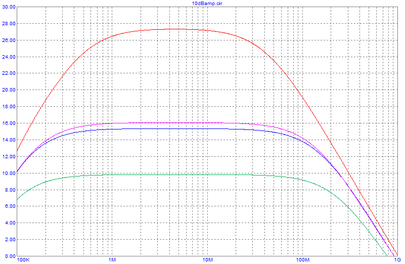
The
red curve is the amplifier's gain without any feedback. The
violet
one is with just emitter degeneration. The blue one is with just
shunt feedback. And the green one is with both feedbacks
working, as shown in the schematic. You can clearly see that feedback
reduces the gain a lot, but also flattens the gain curve, extending the
frequency range over which the gain is essentially constant.
Note
that the gains when using only one type of feedback do not agree with
the ones I calculated above. That's because my calculation was based on
a fixed voltage or current signal at the input, while in the simulation
I used a signal source with a 50Ω internal source resistance. The very
different amplifier input impedances that result from using each
feedback system result in the difference between the simulator's curves
and my calculated values. The situation with both feedbacks enabled
instead shows excellent agreement between my calculation and the
simulator, because it results in an input impedance of almost exactly
50Ω, matching the signal source resistance, so that both calculation
methods agree.
What you cannot see here is how much the
linearity is improved when using feedback. I tried to
get
distortion information from the simulator, by making a Fourier analysis
of the output signal, but the simulator told me that there was
absolutely no distortion ever! Of course... duh!
The
transistor model this simulator uses is a simplified, linear one!
That's the problem with circuit simulators: They idealize the world,
and while some of their output is useful, some other is totally
misleading. Simulators always require knowing beforehand, at least
roughly, what to expect, and then doing a sanity check on anything they
tell. Spice-based simulators are basically linear simulators, and
simulating any nonlinearity is hard for them.
Likewise the
gain curves shown here do not include the effect of all the
imperfections of components and interconnections. How well the gain of
a real circuit will match the simulator output, depends on how
perfectly (free from strays of all sorts) the circuit is built, in
addition to how good the semiconductor models in the simulator are.
In MOSFET
amplifiers it's rather uncommon to intentionally use source
degeneration as a feedback method, due to the high input capacitance
and low voltage gain of these devices. So the feedback is usually
implemented as shunt feedback, but there is alwas also some source
degeneration present, coming from internal MOSFET source resistance.
Since MOSFETs used in an amplifier tend to have a gate-to-drain voltage gain that's quite comparable to the
base-collector voltage gain exhibited by a BJT operating with a typical
amount of external emitter degeneration, we can analyze and
design MOSFET amplifier stages with shunt feedback pretty much in the
same way as we analyze a BJT stage having both forms of feedback.
Although the transconductance of a given MOSFET is variable, depending
on the drain current, and thus causing very nonlinear amplification, we
can usually come close enough by taking the transconductance the given
MOSFET has at the average current it will be conducting.
Let's first consider a simple 3 watt MOSFET HF driver stage that has no
external feedback:
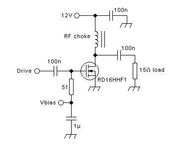
Let's assume that the bias voltage is adjusted so that the MOSFET
conducts an idling current of 1A, allowing it to operate in class A. To
develop 3W into its 15Ω load, we need an RMS output voltage of 6.7V,
and an RMS output current of 0.45A. This equals a peak output voltage
of 9.5V, and a peak output current of 0.63A. Due to both the RDSon of
the MOSFET, and the distortion caused at higher frequencies by the very
strong and nonlinear increase of its drain-gate and
drain-source
capacitances, we can't make it pull its drain all the way to ground,
and the ±9.5V swing around the 12V supply voltage is about the best we
gan get, so the supply voltage is well utilized. Instead it might seem
that biasing the transistor to 1A when only needing 0.63A peak load
current is overkill and wasteful, but look at the published transfer
curve of this MOSFET to see why it is necessary:
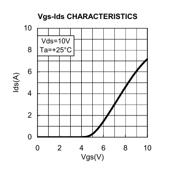
As
you can see, the reasonably linear part of the curve starts at roughly
0.7A or so. In this amplifier the part of the curve being used is the
one that falls between 0.37 and 1.63A, and this already includes some
of the very nonlinear zone! So when adjusting the bias of this
amplifier, one needs to make a compromise decision between linearity
and efficiency. I chose 1A for this example. If instead we bias this
amplifier to only 0.7A or so, its distortion would shoot through the
roof, despite still operating in class A!
Do
you remember the difference I'm making between chokes and RF chokes?
Well... In these MOSFET amplifiers, despite being class A,
which
implies that in principle the supply current is always constant,
allowing the use of any choke without caring about whether or not it
blocks modulation frequencies, we need RF chokes, that pass
modulation frequencies freely. This is simply due to the strong
nonlinearity of MOSFETs. During high amplitude operation the average
drain current over the RF cycle might well differ a little from that at
low or zero amplitude, and the choke needs to accept that current
modulation, or else the drain supply voltage will get modulated by the
envelope signal, causing additional distortion!
For 0.37A
drain current we need roughly 5.2V on the gate, and for 1.63A we need
about 6.1V. So our p-p gate voltage swing is 0.9V, for a p-p drain
current swing of 1.26A, and that gives us a transconductance of 1.4
siemens.
The input impedance of this amplifier is
basically the 51Ω gate swamping resistance, which I also used
to
inject the bias voltage, in parallel with the MOSFET's input
capacitance. This capacitance is the combination of the roughly
constant gate-source capacitance of approximately 47pF, and the Miller
capacitance, which in turn is the product of the drain-gate
capacitance (very roughly 3pF, varying a lot with instantaneous drain
voltage) multiplied by the voltage gain. And this voltage gain is the
output voltage swing (19V) divided by input voltage swing (0.9V), so
it's 21.1. So the Miller capacitance is roughly 63pF, which brings the
total input capacitance of the MOSFET to roughly 110pF. The result is
that the input impedance of this amplifier is 51Ω || 110pF.
Note
that this combination of input resistance and capacitance produces
a pole at 28.4MHz, so the input matching of the amplifier will be
poor at the high end of the HF range. This wouldn't be really
acceptable in an amplifier supposed to be roughly flat to 30MHz. A
lower swamping resistance would be required, to flatten the response to
a higher frequency.
The drive power required is given by the
input resistance and the RMS input voltage. Since the p-p input voltage
is 0.9V, the RMS value is 0.32V, and across a 51Ω load that's only 2mW.
Note that the parallel input capacitance doesn't require any additional
drive power, but just additional drive current, which is 90° out of
phase with the drive voltage! Of course a typical driving source would
have trouble with this additional out-of-phase current. Anyway, since
the amplifier produces 3W output, the gain is a whopping 32dB! But the
frequency response is poor, and the linearity too.
Let's fix the
input first. By quadrupling the load on the gate, we push the problems
4 times up in frequency, which should be good enough. If we want to
keep a ~50Ω input, we then also need to add a matching transformer:
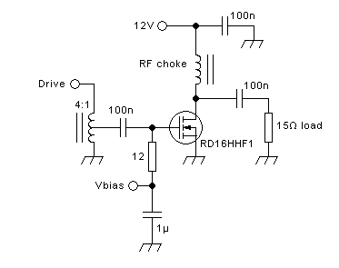
Now
the input impedance is 48Ω || 27pF, giving us an input pole frequency
of roughly 114MHz, which is fine for HF use. But it came at a
price! Not only the added autotransformer, but also we now need twice
the drive voltage, four times the drive power, and this means that the
gain of the modified amplifier is 6dB lower. That's still a gain of
26dB, which is pretty good, and might actually be too much in some
applications.
But now lets finally introduce intentional shunt
feedback, in parallel to the capacitive shunt feedback that's always
present due to the drain-gate capacitance of the MOSFET. Let's
arbitrarily replace about 90% of the gate swamping by shunt feedback:
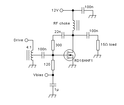
As
you can see, I increased the value of the swamping resistor tenfold,
and added shunt feedback. Since the voltage gain of the amplifier
(given by MOSFET transconductance and load resistance) is
21.1,
and the output voltage is in phase opposition to the drive voltage, the
total RF voltage between drain and gate is 22.1 times the drive
voltage. So the value of the feedback resistor needs to be
22.1
times higher than the part of the swamping resistor it replaces. Since
that one is about 13Ω (because 13Ω in parallel with 120Ω is roughly
12Ω), we need close to 300Ω of shunt feedback resistance. A DC blocking
capacitor of course needs to go in series, and its value needs to be
large enough to keep the feedback functional down to a sufficiently low
frequency.
Now the drive current splits about 10% into the
swamping/bias resistor, and 90% into the feedback resistor. What did we
gain by doing this? Well... errr... blush... nothing,
so far! In fact we have added two parts, we are now wasting some of our
output power into the feedback resistor, but the drain signal current
still depends strictly on the drive voltage, which depends on the
driver! So does the distortion, frequency response... really so far
there is no improvement!
Of course this changes when we factor in the
internal resistance of our signal source. Let's do that
explicitly:
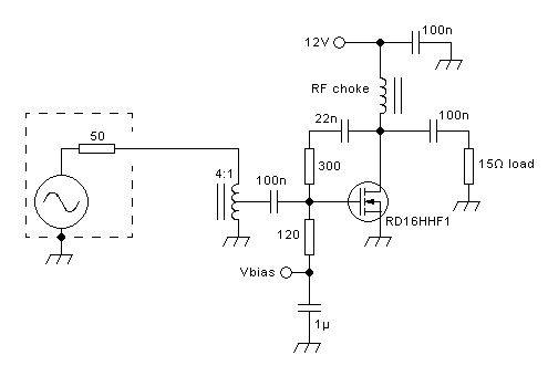
Assuming
that the 4:1 autotransformer works as it should, and that the coupling
capacitor is transparent at RF, the 50Ω internal resistance of the
signal source, transformed down to 12.5Ω by the
transformer, forms
a voltage divider with the impedance at the MOSFET gate, which is the
parallel combination of the 120Ω swamping and bias injection resistor,
with the 300Ω feedback resistor divided by the voltage gain plus
one, the MOSFET's gate-source capacitance, and the drain-gate
capacitance multiplied by the voltage gain plus one.
Now we do
get a benefit from having mostly replaced pure dumb gate swamping
by feedback: Lower distortion! Because any distortion products
appearing at the drain will feed back into the gate, and will actually
be able to alter the gate voltage, which is no longer firmly tied to a
stiff voltage source in the form of a zero impedance driver. This
causes an
opposing drain current change, attenuating that distortion. Also any
gain reduction at high frequencies caused by runtime effects in the
transistor, or by source lead inductance, will also be moderated,
resulting in some extension of the flat gain range.
It's
interesting to understand what source impedance the gate itself sees,
over the frequency range. In the normal operating frequency range,
where the transformer works fine and the MOSFET too, this is the 50Ω
drive source resistance, transformed down to 12.5Ω by the transformer,
in parallel with the 120Ω bias injection/swamping resistor, in parallel
with the roughly 13.5Ω of effective resistance provided by the feedback
circuit. That makes a total of roughly 6Ω.
But at
very low frequencies this condition falls apart: The transformer no
longer works well, making it look like having a parallel low value inductor to ground. At the
same time the coupling capacitor no longer has near-zero impedance.
This forms a pretty series-resonant circuit from the gate to ground,
which interacts with the internal MOSFET capacitances, so that we get a
series and a parallel resonant frequency! It's very easy to unwillingly
build an oscillator in this way! Negative feedback should help prevent
oscillation, but our negative feedback path also becomes capacitive at
those very low frequencies, as the 22nF capacitor's
reactance starts to dominate over the 300Ω resistor. The
parallel
resonance at the gate still gets loaded and thus de-Q-ed by the
swamping resistor, which is connected to the bias source, which
hopefully has a low impedance down to DC. But that doesn't help with
the series resonance, which can still make the circuit oscillate! We
typically need to load and de-Q that one too, by adding a small
resistor in series with either the gate or the coupling capacitor. More
about this sort of trouble comes in the chapter about amplifier
stability! For now I will just suggest that by
adding
this series resistance our amplifier not only gets more stable, but
also gets more independent of the signal source's internal impedance.
In an extreme case we might want to put in a series resistance
so
large that it provides matching to the driving source, without needing
the transformer:
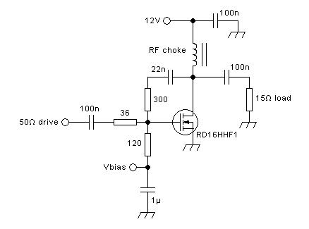
The 50Ω input resistance is now
given by the 36Ω resistor in series with the effective 12Ω of the
swamp+feedback combination. The cost of this is that we need
to
again double the drive voltage, quadruple the drive power, and thus the
replacement of the transformer by a resistor costs us another 6dB of
gain. But it provides excellent stability, combined with a good gain
flatness, and reasonably low distortion, and the mentioned moderate
degree of independence from the driving source's internal impedance.
The
voltage gain of this amplifier would be about 5.5. The current gain is
about 18, given that the load resistance is much lower than the input
resistance. That's a power gain of 100, which is 20dB. Not bad!
In the most recent Blue Block, way above, I told you about the two
modes of push-pull
amplifiers, and I hinted that they apply to feedback too.
It's time to look deeper into this.
This circuit
shows the input and feedback configuration of a push-pull amplifier
built as two separate amplifiers in opposite phase:
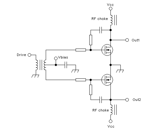
As
you can see, the two sides are totally independent, each with its own
shunt feedback and series resistor. The only element joining them
(apart from ground and Vcc, of course) is the drive transformer, whose
secondary's center point is grounded for RF and modulation frequencies
(the latter thanks to a low impedance bias supply). The drive
transformer then forces equal and opposite signal voltages
driving
the two gain sections. As long as the resistor values are chosen such
that they force a voltage gain that is much lower than the voltage gain
resulting from the MOSFETs' transconductance and the load impedance
value, each of the MOSFETs will produce a well-controlled output
voltage, equal in magnitude and of opposed phase, to be
delivered
to any sort of output transformer.
In this way this circuit
implements full feedback: There is both differential-mode and
common-mode feedback. This can be easily seen by playing the "what if"
game: What if the instant output voltage difference is less then it
should? In other words, if the output differential voltage is
too low? Well, the feedback circuit will make both gate voltage
change in opposite directions, such that the error gets
largely
corrected. And what if both outputs go too high, together? That is, a
common-mode output voltage appears? Well, the feedback circuit will
then pull both gates a little higher, largely correcting that
common-mode deviation.
Now let's modify that circuit, adding a feedback transformer:
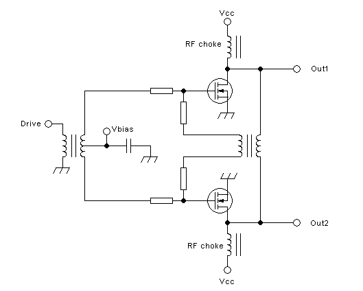
This
is a pure differential-mode feedback. Any difference between the two
output voltages creates an output from the feedback transformer, which
is applied differentially between the gates. Instead any common-mode voltage on
the drains is simply not seen by the transformer, causing no feedback.
Usually the
secondary winding of the feedback transformer has far fewer turns than
the primary, often just a single turn. This allows
reducing
the value of the feedback resistors, and specially, reducing the power
loss in them. This is an important advantage in amplifiers powered from
relatively high voltages, which tend to require high power RF resistors
when using direct drain-gate feedback. Anyway this reduction of power
wasting is a poor reason to choose differential-only feedback, because
there is no reason why it should be impossible to use two separate
feedback transformers, thus implementing full differential and
common-mode feedback, combined with low power loss in the resistors. But
the circuit is more complex, with one additional transformer and
several additional capacitors, so it's rarely done.
Differential
feedback is fully capable of controlling the amplifier's differential
gain, reducing the distortion of the differential output voltage, extending the
flat gain bandwidth, but it does nothing to keep each drain voltage
centered around Vcc! At DC, and up to the frequency where the RF chokes
start becoming effective, the RF chokes will force that centering, but
not at RF. So it's very possible, and even quite usual, that an
amplifier configured like this will show totally different, asymmetric,
extremely distorted drain voltage waveforms - but the
differential
voltage, from drain to drain, will still be reasonably clean!
The
problem is that as one transistor saturates, while the other
compensates for that, inevitably there will be some additional
distortion in the output, and often one transistor will heat up more
than the other one, possibly leading to thermal run-away.
What's
even worse, this amplifier will exhibit extremely high and uncontrolled
common-mode voltage gain. Any signal leaking into the gates, such as
capacitive coupling between the feedback transformer windings, will
appear in common-mode at both gates, causing common-mode drain
current. Also any common-mode signal created by the MOSFETs themselves
when driven differentially, due to their nonlinearity, will do this.
Since the drains aren't loaded for common mode, due to the load
being connected differentially, a very large common-mode drain voltage
signal results. It might easily exceed the drain voltage limit, making
the transistors go into avalanche conduction, which can easily destroy
them. And last but not least, such a high, undesirable, unneeded
common-mode gain could very easily cause the amplifier to oscillate in
common mode.
All this said, I should again mention that neither this
amplifier, nor any amplifier, is completely free from direct drain-gate
feedback. The reason is the drain-gate capacitance of the MOSFETs,
which is quite important at the higher frequencies, even becoming the
dominating factor. But at lower frequencies this internal feedback path
gets less effective. Also, being a capacitive path, the feedback it
provides is 90° out of phase, doing half of the job required to make an
amplifier oscillate! If the other half comes from phase shifts in all
other circuit parts, we get a low-frequency oscillator instead of an
amplifier.
Even so, this transformer-based differential feedback
circuit is very often used in commercially made radios! Some of that may even be
due to designers not fully understanding what they are doing. But their
are indeed ways to get such an amplifier under control even in
common-mode. Remember the chapter about feed configurations for
push-pull amplifiers: By using a bifiliar feed choke, balanced feed
transformer, or whatever you want to call it, the drains are forced to
carry mirror images of any signal present, and that shorts out any
common-mode voltage at the drains! When there is no possibility of
common-mode drain voltage, there is also no need for any common-mode
voltage feedback. Also a dedicated feedback transformer becomes
unnecessary, because a simple, single turn on the feed choke can be
used in its place. This is very commonly done, and looks like this:
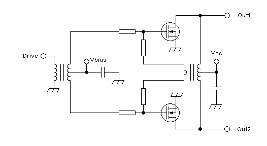
Very
simple, nice, and cost-effective. That's why manufacturers love
to use it! Also this circuit allows true class AB and class B
operation, unlike the amplifier using separate chokes, which is only
good for class A, dynamic class A, and current-switching class D. There
is just one problem, and it's a big one: The extreme difficulty in
making such a coupled feed choke that actually maintains good coupling
to the highest frequencies required, and in physically building the drain-feed-bypass circuit with low enough stray inductance.
In theory it would also be
possible to use a single transformer for the whole drain feeding, load
matching and feedback business. But in this case the difficulties are
even greater. At power levels of about 100W and greater, with the
typical low supply voltages used, the leakage inductance becomes
impossible to manage even
in the mid HF range, let alone its high end. I have never seen an
amplifier in this power class using such a do-it-all transformer.
If a designer ever
wanted to implement only common-mode feedback, without any
differential-mode feedback, it can certainly be done, such as
in
this example:
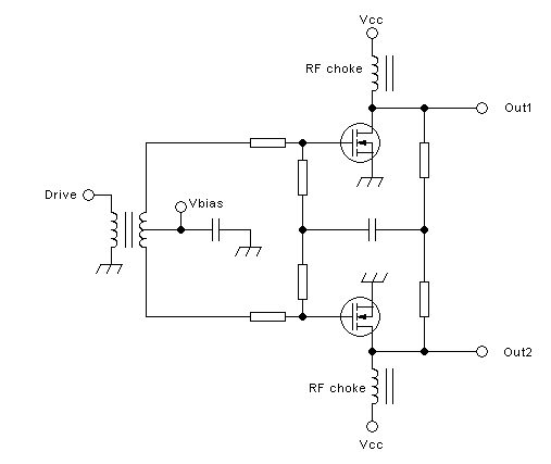
The
two resistors connected to the drains react purely to the common-mode
drain voltage, and this is applied in the same phase to both gates. The
common-mode gain can be controlled by the resistance values, while in
differential mode this amplifier operates in open loop.
The main problem with this circuit is that no matter how hard I think,
I can't come up with a good use for it!
Let's
instead make a small modification that allows implementing a stronger
common-mode feedback than differential-mode feedback. Such a
configuration is useful if we want to forcefully keep the drain
voltages from developing any significant common-mode signals,
while having a weaker differential-mode feedback in order to still get
enough gain. I will base this circuit on the one that has two
completely separate sides, with just one small modification:
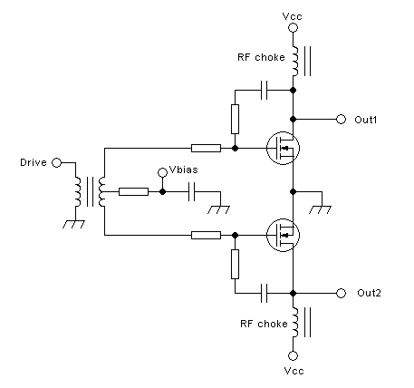
The
modification is, obviously, adding a resistor in series with the drive
transformer center tap. The differential feedback still depends just on
the ratio between the shunt and drive series resistors (including the transformed impedance of the driver), while the
common-mode feedback depends on the ratio between the shunt resistors
and the series combination of the gate series resistors and the center
tap resistor.
If this new resistor is replaced by an RF choke,
the common-mode feedback becomes extremely strong, forcing essentially
complete absence of common-mode signals at the drain. But the reactance
of the choke is a stability hazard in the frequency range where the
choke starts becoming ineffective.
Note that if a drive
transformer with a single secondary turn is used, as is often the case
in large amplifiers, the center tap is essentially uncoupled, so it
behaves like a series choke! So this amplifier has very low common-mode
gain:
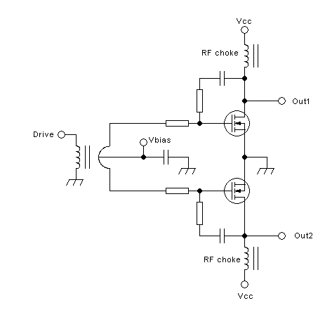
Such
transformers are deceiving, because many people people assume that
their center tap actually works at RF, which it really doesn't!
The same effect can be achieved by using no center tap at all, and
injecting the bias voltage through a high value resistor:
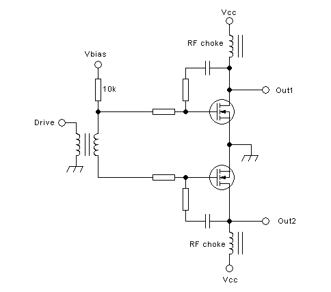
This
circuit might look crazy, because the bias is injected into just one
side. Of course this really doesn't matter, because the drive
transformer has essentially zero DC resistance, and the bias resistance
I chose is so high that the RF imbalance it causes is totally
negligible, at least as long as the driver used doesn't have
near-infinite impedance.
But if you build a circuit like this, and you want perfect symmetry,
just for the aesthetic value of it, then I gracefully allow you to use
two bias resistors, one to each side...
The advantage of this
configuration over the one that has a resistor at the center tap is, of
course, that no center tap is required, simplifying drive transformer
construction. This may be particularly important when using a transmission-line transformer for driving.
An amplifier like this works with purely
differential drive, optimal differential feedback, and very strong
common-mode feedback. It forces a good balance between sides, despite
having no direct drain-to-drain coupling. But one needs to
use
great caution when designing such an amplifier, because there is a trap
built in: The common-mode gate voltage can be pulled and pushed very
heavily by the feedback, possibly destroying the MOSFETs by exceeding
the negative gate voltage spec! Getting too high a positive gate voltage is
impossible, because when the gate voltage goes pretty high, the MOSFET
conducts so strongly that it pulls down its drain, no matter what, and
thus limits the positive gate voltage excursion. The problem is just
with negative gate voltage. If for any reason
both drain
voltages are pulled down fast, the gates follow that, the MOSFETs turn
off, and since they can't turn "offer" than off, they cannot keep the
gate voltage from going strongly negative. In amplifiers operating
from 12V, and using VDMOSFETs with their ±20V or even ±30V gate
voltage ratings, this doesn't pose any risk, but with 50V-powered
amplifiers using LDMOSFETs having a gate voltage rating of perhaps
+13/-6V, damage can easily happen. So it would be wise to either not
use a circuit with such strong common-mode feedback in 50V LDMOSFET
amplifiers, or add gate voltage clamps that will prevent excessive
negative gate voltage spikes.
Increasing the common-mode
feedback strength is very useful for controlling drain voltage
overshoot. You may remember what I explained about push -pull amplifier
feed arrangements in the section about output circuits, way up
this page, and in the Blue Block comparing Dynamic Class A
to Linear Class D. The main point is: When there is any
significant uncoupled inductance in the supply path of each drain, this
inductance tries to keep the supply current constant throughout the RF
cycle, but a class AB amplifier needs to vary that current from almost
zero to maximum, twice per RF cycle. So the two requirements clash, and
the result is extremely high inductive voltage spikes on the drains,
which at best only create distortion and lower efficiency, and at worst kill the transistors. A
feedback scheme that implements very strong common-mode feedback, like
the ones we were just looking at, can largely control this
problem. Whenever the MOSFETs try to suck more current than the drain
chokes are carrying, the common-mode drain voltage will sag, and this
will reduce both gate voltages, limiting the current drawn by whichever
MOSFET is conducting at that time. Likewise, when the drive signal is
crossing zero, so that the MOSFETs would have just the bias voltage on
their gates and conduct very little current, but the drain chokes are
still forcing in the same high current as before, the common-mode drain
voltage would soar. In even clearer words, both drains would see a very
dangerous high voltage spike, at the same time. With strong common-mode
feedback, this won't happen, because both gates will be pulled up,
enabling both MOSFETs to conduct the current standing in the chokes. So,
by using strong common-mode feedback, we turn a class AB amplifier with
dangerous high voltage spikes on the drains into a dynamic class A
amplifier, that is largely free from these spikes! The price we pay is
that we get a full-power efficiency more like that of a class A amplifier, than a
class AB one. But at least the idling current follows the signal
amplitude, and during modulation pauses the dissipation is as low as in a class AB
amplifier.
In this way feedback can have a strong effect on bias, despite
there being no DC feedback path, and not even a low-frequency feedback
path!
We can also employ feedback to implement frequency
response compensation.
With BJT amplifiers this can be quite important, because
many
BJTs used for amplifiers operating in the HF frequency range have an Ft
of just 100MHz or little more, so their current gain drops with
increasing frequency at a steady rate through most of our intended
operating frequency range. The gain would be very much lower at the
high end of the range than at the low end. Proper compensation
for this can be included in the drive path, or in the feedback path, or
even in both of them. Since this involves inserting reactive
components, such as inductors in series with the shunt feedback
resistors, great care has to be used to make sure the amplifier remains
stable. The general idea is to reduce the strength of the negative
feedback as the frequency rises, to compensate for falling gain in the
transistors. This also tends to keep the input impedance more constant,
since the base or gate impedance of transistors drops with increasing
frequency.
MOSFETs used at HF have a much flatter
frequency response, because their Ft is so high that usually we don't
need to worry about it when operating at HF. But their input impedance
drops even more strongly with frequency than that of BJTs, and this is
one of the limiting factors to a MOSFET's practical operating frequency range in a
broadband amplifier. Not so in a tuned amplifier, where the
capacitances can mostly be tuned out. That's why a given MOSFET might
work well in a tuned 200MHz amplifier, while being suitable only for up to
50MHz or so in a broadband amplifier.
Given the high gain of
LDMOSFETs, usually we can get enough gain flatness by simply using
plain simple feedback, strong enough to lower the gain so much that our intentional
feedback controls the gain throughout the frequency range, rather than
the internal drain-gate capacitance. And we also either swamp the input
capacitance of the MOSFETs through strong feedback, or we can help the
situation by absorbing it into a lowpass filter section, as explained
in the chapter about driving. Again, this involves reactive elements,
and care must be used to avoid instability.
And since I have been writing so much about stability and oscillation,
it's time to begin a proper chapter about it!
Amplifier stability
Let's begin with Murphy's Law of Amplifier Stability: Any amplifier that can
oscillate, will oscillate. There are several extensions
and additions to this law. For example: An amplifier that is
conditionally stable will start oscillating at the worst possible time.
That might be precisely when you demonstrate your
amplifier during
an international symposium about RF design, or while an EMC inspector has his spectrum analyzer
connected to it. Amplifiers that go into satellites will start
oscillating precisely when they reach orbit, never earlier.
There
is also a combinational extension to this law: When you connect a
stable driver to a stable final stage, the combination will oscillate.
There is even a corollary that applies to individual components: Whenever
an amplifier gets damaged from oscillation, the most expensive and
hardest to replace component is the one that will fail. A
sub-corollary to this is: The
likelihood that an RF power transistor will be destroyed during
oscillation is directly proportional to the cost of that transistor.
So
we clearly need to take all required measures to make sure that our
amplifiers just cannot oscillate, no matter how hard they try. There should be absolutely no
condition, not even the least likely one, that could result in
oscillation. But this, my dear readers, is much easier to write or say,
than to achieve!
Let's review the theory of oscillators: It
simply says that any device that has feedback will oscillate, if there
is any frequency at which the feedback is exactly in phase, and there is enough
gain to overcome the losses in the entire feedback loop. So you need
just three things to get oscillation: Gain, feedback, and a suitable
phase of the feedback.
Any amplifier has gain, or it wouldn't be an amplifier. So we can't
attack oscillations by eliminating gain, at least inside the required operating frequency range. One out, two to go.
You
might think that it would be wisest to avoid building feedback into an
amplifier, to prevent oscillation. Unfortunately this isn't possible,
because there is always some feedback. Every transistor has shunt
feedback through the drain-gate or collector-base capacitance, also
there is always some feedback through the impedance of the emitter or
source connection, and there is additional feedback through capacitive
and inductive coupling between the input and output circuitry, and by
feedthrough on the power supply line into the bias supply, and into the
main supply of the other stages in an amplifier chain, and, and, and... So, feedback is
unavoidable, and instead of going to extremes in fighting it (called "neutralization"), it's very
often easier and better to overwhelm the inevitable undesired feedback with strong,
intentional, correctly designed feedback. One more out, just one to go.
And
that's the phase of the feedback. In any amplifier, or chain of
amplifier stages, we must make absolutely sure that under no condition
there is any frequency at which the phase of the feedback is the
correct one for oscillation, while at the same time there is any gain
in the loop. This is the golden rule of stability!
The phase
required for oscillation, of course, is such that a signal applied to a
point of the loop gets amplified, fed back, delayed, inverted, inverted
again, shifted forward, shifted back, whatever, and ends up returning
to that same spot in the exact same phase as it was injected. It
doesn't matter whether it's phase shifted by 0°, 360°, 720°, or even
more full periods. Any of those is good for oscillation.
When we
design an amplifer, in principle we apply negative feedback, that is,
the feedback is 180° shifted from the original signal. That's a simple
phase inversion. At least that's our first goal. Inevitably there will
be some additional phase shifts, forward or backward, that make the
feedback phase angle deviate from the optimum 180°. Our second goal is
to keep the combination of all these shifts under control, in such a
way that there is no frequency where they add up to an additional 180°
shift, which would put the feedback signal in phase with the drive, and at which there is still gain.
A
feedback loop will self-oscillate only when the total phase shift is
exactly right. The oscillation will automatically happen on the
frequency where this perfect phase shift happens. That's why oscillators can be
tuned by varying a capacitance or inductance, after all. If there is no
frequency where the correct phase shift happens, there will be no
self-oscillation, but when the phase shift is close to the required
one, the amplifier will ring.
This means that when excited near that frequency, or with a pulse that
contains all frequencies, this will kick-start an oscillation at the
resonant frequency, with an amplitude that decreases over time until
fading into the noise. The closer the phase of the feedback is to the
critical one that causes self-oscillation, the stronger and longer will
be this ringing. Likewise, the higher the loop gain is, the more
ringing will occur.
How much ringing is acceptable, depends on
the application. A rule of thumb that's often used is that the designer
should keep at least ±45° of phase margin, ideally ±60°, and at least
6dB of gain margin, ideally 10dB. Translated into a slightly more
human-compatible lingo, it means that the total phase delay, including
phase inversion, along the complete feedback loop, must be anywhere
between 45° and 315° at all frequencies where the loop gain is at least
unity, and at any frequency where the total phase delay is 0°, the loop
gain must be ≤ -6dB. And if
you
can get the delay to fall between 60° and 300° at all
frequencies
where the loop gain unity or higher, and the gain to be ≤ -10dB at any
frequency where the phase is at 0°, you can call it an excellent
result. These numbers don't need to be super precise. When comparing
signal amplitudes on a scope screen, it's plenty accurate enough if we
consider 6dB to be a ~2:1 voltage ratio, and 10dB a ~3:1 ratio.
Of course it's almost impossibly difficult to calculate
the phase shift and gain for every frequency, in an amplifier that has
many unknown values, such as varying and poorly specified internal
capacitances of transistors, unknown wiring inductances, and
ferrite-cored chokes that vary their inductance and loss in a non-linear way
according to the current flowing through them. I often do just some
educated guesses to determine whether there is an obvious problem in my
design, or if it seems to be on the safe side. Then I try it. This is
really tickling Mr. Murphy and asking for trouble, but with some care
it works, and is much more fun than filling 50 sheets of paper with
extremely complex equations - and making one maths mistake that messes
up the whole calculation and gives a totally wrong result!
Enough said about the theory. Let's see
how it's done in practice, by analyzing the stability of a real
amplifier. For simplicity, let's use one of the examples I used in the
previous section:
Let's
assume that the RF choke has a value of 22µH, that the 12V
and
bias sources have zero internal impedance, and that the drive signal
source has a 50Ω internal impedance, free from reactance.
To
start, imagine what happens if there was a signal of 1mV on the gate,
at 2 MHz. We calculated way above in this page that this
transistor, operating at an idling current of 1A, has a
transconductance of roughly 1.4S. Thus the 1mV gate signal will cause a
1.4mA drain current signal. At this low frequency, the delay
in
the MOSFET is negligible, so we can consider the drain current to be
precisely in phase with the gate voltage. But the current is sunk
rather than sourced, so it's actually 180° out of phase. Since this
phase inversion isn't associated to time delay, it makes the same sense
to consider it positive or negative. For the fun of it, let's consider
it to be -180°.
To calculate the
resulting drain voltage signal, we need to calculate the total
impedance seen by the drain. This is the result of the 15Ω load in
series with the 100nF coupling capacitor, in parallel with the 22µH of
the choke, in parallel with the series connection of the 22nF and the
300Ω, with the added complication that this latter branch does not
return to the RF ground, but the the 1mV gate signal point, and at this
moment we don't even know the phase difference between the drain and
gate voltages!
This is too complex to be practical, so let's
make the approximation of considering 1mV to be negligible. This is
quite daring, but let's try to get away with it. So we have 3 branches
in parallel, two of them composed by resistance and reactance, and to
this we must add the two internal branches of the MOSFET: The
drain-source capacitance, and the drain-gate capacitance, where the
latter again requires either considering or neglecting the 1mV gate
signal! To put the cherry on the pie, these two capacitances vary like
crazy during the signal period, and also their averages over the period
vary with amplitude... But hey, we are doing small-signal
analysis here, so let's consider them constant!
You see, the matter is complex, and we need to make practical
simplifications to ever get anywhere.
Resolving
this network of impedances at the drain, which can be done by hand and
calculator, or using software, or even using online calculators, I get
14.3Ω at a phase angle of -0.3°. Which means that at this frequency the
reactances in the circuit have a very small effect, and largely
compensate each other. The resulting impedance is almost exactly just
the 15Ω load in parallel with the 300Ω feedback resistor.
This
makes things nice and easy. The 1.4mA drain signal current, when
applied to this impedance, creates a drain voltage signal of 20mV. The
phase of this voltage signal is -180.3°. Great.
Now let's see
what the shunt feedback does to the gate voltage, to complete the
loop: 300Ω in series with 22nF is an impedance of 300.02Ω at
a
phase angle of -0.7°. A negligible difference from a pure 300Ω
resistor. Let's add the drain-gate capacitance of the MOSFET, about
2.2pF, in parallel. The result is a tad less than 300Ω, at -1.2°.
Due
to the almost exact phase opposition between gate and drain voltages,
there is 21mV across the 300Ω, which injects a current of
70µA
into the gate note, at a phase angle of -179.1°. That's because
dividing a voltage by an impedance that has a negative phase shift
results in a current with a positive phase shift, so the phase is
-180.3°+1.2°.
This current sees 3 parallel paths to ground.
One is the gate-source capacitance of the MOSFET, 55pF. Then
there is the 120Ω bias resistor, which is RF-grounded at the other end,
and the series combination of the 36Ω input resistor, the 100nF
coupling capacitor, and the 50Ω internal resistance of the drive
source. Resolving this network, I get almost exactly 50Ω, at -2.3°.
70µA in 50Ω makes 3.5mV, and the phase current of -179.1° in an
impedance of -2.3° makes a voltage phase of -181.4°.
So,
the loop gain of this amplifier at 2MHz, under the conditions shown and
assumed, is 3.5 (a little more than 10dB), with a phase shifted only
-1.4° from perfect negative feedback. This is very good, and
there
is not the faintest chance of any oscillation at 2MHz.
One
could do a stability analysis by putting all these calculations into a
little program, or even a spreadsheet, and having the computer
calculate the loop gain and phase for a very wide range of
frequencies, from 1Hz to 1GHz or so, and make sure that the
conditions for oscillation don't happen at any frequency, and that the
phase and/or gain margins are OK. Or if you are fluent using a circuit
simulator, this is a great opportunity to use it, but you need to use
it carefully, because transistor models in simulators are often very
poor, and lead to wrong results. I prefer simulating just the passive
circuitry in my simulations, and add myself what I assume the
transistor should be doing.
I put a passive model of the feedback circuit into Micro-CAP:
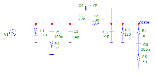
The
signal source is configured to create 1.4kV, with a 1MΩ internal
resistance, to create a pretty well defined 1.4mA current injection
into the circuit. This simulates the drain current signal created
by 1mV on the gate. L1 is the supply choke, C1 the output
coupling
capacitor, R1 is the load, C2 is the MOSFET's drain-source capacitance,
C4 its drain-gate capacitance, C5 its gate-source capacitance. C3 and
R2 are the shunt feedback parts, R3 the bias resistor, R4 and
C6
the input parts of the amplifier, and R5 is the official signal
source's internal resistance.
Then I made a sweep from 10kHz
to 1GHz, to create a Bode plot (gain and phase) of the feedback loop. I
adjusted the gain scale to correct for my crazy current source and the
transistor's gain, and I added the 180° phase shift occuring
in
the transistor. This is the result:
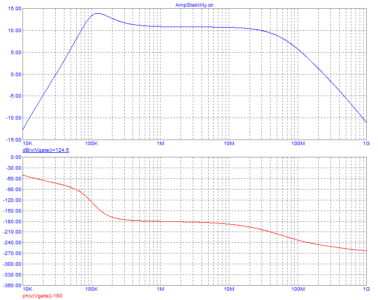
In
the desired operating frequency range, from 1.8 to 30MHz, the feedback
is of pretty constant strength, and its phase drops from the nominal
-180° to about -200°, so it's excellent negative feedback through that
whole range.
In the low frequency area we see a gain peak,
then a fall-off, along with the corresponding phase shift. Unity loop
gain (0dB) is reached at 30kHz, and the phase margin is about 72°,
which is excellent. The frequency at which the feedback loop reaches
zero phase is way out of the graph, and the loop gain at that frequency
is way below unity, probably -20dB or even more down, so the gain
margin is very ample. There is no risk of low frequency
oscillation.
At the high frequency end this Bode plot is not
accurate, because it does not include the effects of the transistor's
internal delay and gain drop. This data isn't given in its datasheet,
so I have to go by feeling and experience, or else built a test setup
and measure this MOSFET's behavior. Anyway, without including the
VHF/UHF effects contributed by the MOSFET, this amplifier has an
excellent stability profile, with a unity loop gain crossing
at
roughly 230MHz, and a phase margin of about 110°. When the roll-off of
the transistor is added, this will get worse, but hopefully
not
nearly enough to make the amplifier oscillate at VHF.
So there is a good chance that this amplifier will be unproblematic.
But
I was analyzing it under optimal conditions! A clean resistive load,
and a signal source with a constant, clean internal resistance. In
practice this is very often not so, and depending on what load the
amplifier has to drive, and what impedance the signal source has, the
picture could be quite different! For a real application, we need to
simulate the loop gain and phase under the actual operating conditions,
with the true load and true signal source connected.
Let's use
the simulator to play the "what if" game. First test: Remove the load,
let the amplifier run unloaded. The Bode plot changes to this:
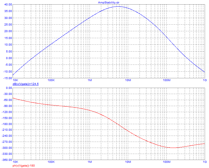
Note the change of scale in the gain graph! There is a very high loop
gain around 6MHz, but it's no problem, because the phase stays close to
-180°. At the low-frequency end there is no change, because there the
very low impedance of the supply choke dominates over the load, or the
lack of it. But watch the range around 100MHz: The phase margin is only
60° with a loop gain of 10 to 15dB, which is no problem by itself, but
after adding some additional phase delay in the MOSFET, things could
get tight here! There is some risk that the phase might drop
all
the way to -360° before the loop gain has dropped to 0dB, and in that
case the amplifier will do what amplifiers love more than
anything: Oscillate!
So, in case that the application of this
amplifier might include an open-load situation, it would be wise
to find out the transistor's time delay and gain curve, and
include it in the simulation. Another possibility is just building the
amplifier and testing it without a load, at various supply voltages,
bias settings, temperatures, and see if it does any mischief. If it
oscillates, the frequency would be somewhat lower than 100MHz. If it
doesn't oscillate, it would be good to inject a small signal, sweep it
over the suspect range, and see how much the amplifier rings.
And what happens if we short the load? Just see:
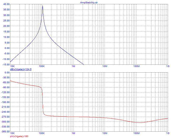
We
get a nasty, sharp resonance near 100kHz, because the feed choke and
the output coupling capacitor form a parallel resonant circuit at the
drain. The phase changes through almost 180° in a very small frequency
span. But still there is no problem, because the phase margin on the
low end is essentially unchanged at about 72°, and on the high side
it's slightly over 90°, at only 400kHz, where the MOSFET adds almost no
delay. So there is no risk of oscillation when shorting the load.
And
what happens if the load is purely capacitive? Well, that depends on
the capacitance value. Let's try 500pF, and see what happens:
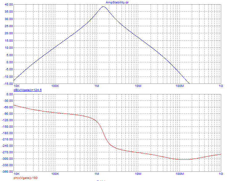
The
resonance moves up, and broadens. It's simply an intermediate case
between the shorted load, and the open load. We need to begin watching
what happens when adding the transistor's delay.
And what if the load is inductive? Let's try with 1µH:
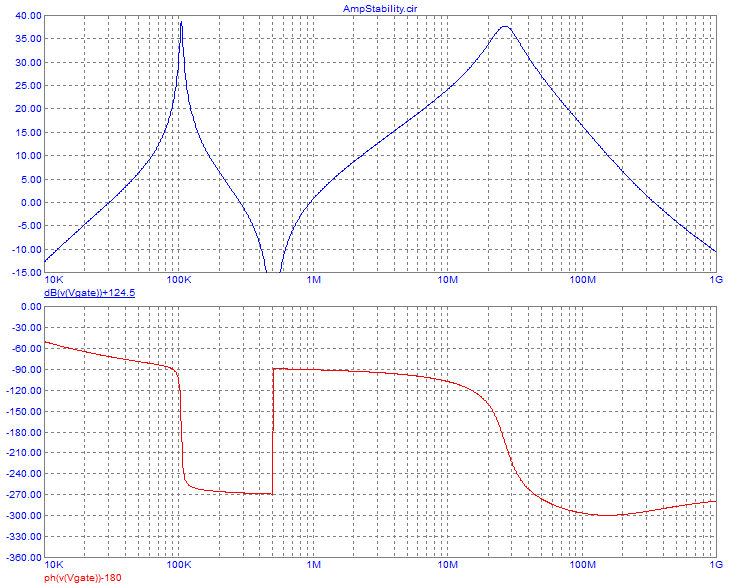
The
plot turns pretty wild! The inductive load forms a series resonant
circuit with the coupling capacitor, at 500kHz, while at 100kHz
this inductance turns quite insignificant, acting as a short and
allowing the coupling capacitor to form a the same parallel circuit
with the feed choke as it did before. The important point, for
stability purposes, is that the phase margin is still about 72° at the
gain zero-crossing frequency of 30kHz, so there will be no low
frequency oscillations, and that around 100MHz we still get some risk
of oscillation, if the transistor adds significant delay there, which I
don't know.
Then I returned to the normal resistive load, and
instead changed the driving source to have infinite internal impedance.
This is what you would approximately get by using a driver stage that
has no shunt feedback:
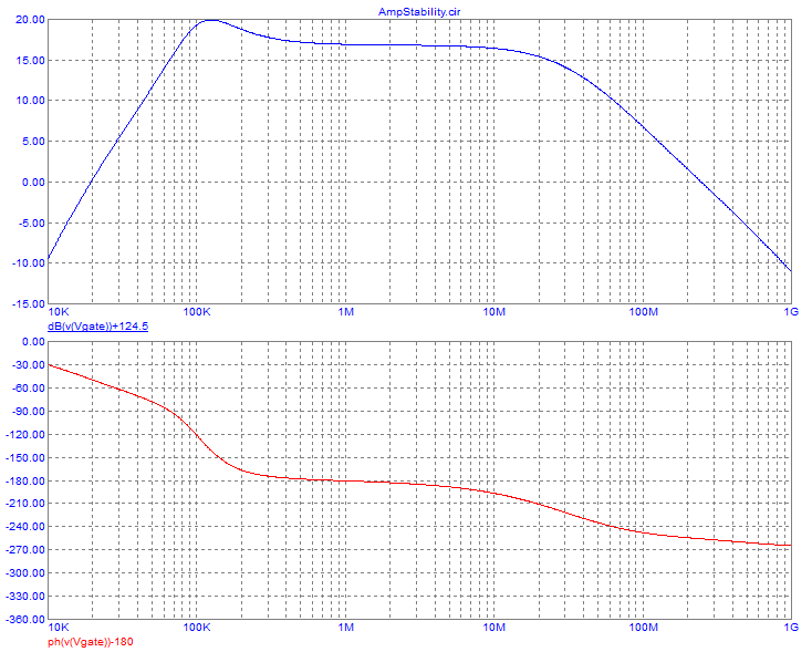
Note
the change of scale again. And note that due to the lower loading of
the gate circuit, the whole loop gain curve is higher, resulting in the low
frequency 0dB crossover shifting down to 20kHz, with a phase margin of
only 50°. This is still OK, but approaching the acceptable limit. On
the high frequency side instead there isn't much of a problem, with a 0dB gain
transition at about 240MHz, and a phase margin of about 100°, which
gives room for quite some delay in the transistor, without anything bad
happening.
And then let's try a driving source with zero
internal impedance. An RF operational amplifier would have that
behavior, and also a transistor driver using very strong shunt
feedback. An emitter follower stage can also approximate that behavior.
What we get is:
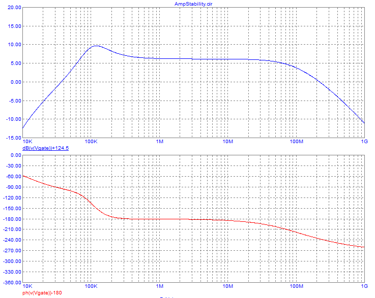
It's
a very benign curve, with phase margins better than 90° on the low
side, and about 120° on the high side. This shows that using strong
shunt feedback in each stage of an amplifier chain can be a very good idea! The 36Ω
input series resistor, grounded through the zero driver impedance,
gives us this advantage. A low gate swamping resistor to ground would
do the same for a high-impedance driver. Of course, it would reduce
the amplifier's gain too.
Now I will show you examples of what
really makes amplifiers oscillate!
There are so many pitfalls that I can only mention a few, to
give
you an idea. First example: Let's suppose that there is this new ham,
who is learning to build radios. He bought an RD16HHF1 transistor, and
wants to build an amplifier with it. He doesn't want the complexities
of band-switched low-pass filters, and in fact he doesn't fancy
multiband
operation at all, in addition he lives in a country where getting
ferrite cores is hard, so he decided to make a tuned amplifier, just
for the 40m band.
Since he knows that tuned amplifiers are prone
to oscillating, he decides to be very careful to avoid feedback paths.
He installs very good power supply decoupling, bias supply decoupling,
and he avoids using shunt feedback, for fear that the negative feedback
will end up turning into positive feedback at some frequency. He even
is so careful as to add a shield between the input and output
circuitry, to prevent any coupling between the tuned circuits. The
result of his effort is this:
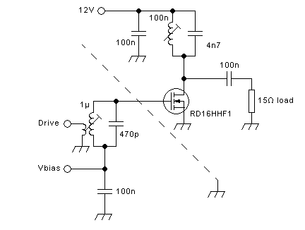
He builds the circuit
nicely into a shielded box, and as soon as he connects the power supply and bias, he gets a
strong, solid carrier at the output, right in the 40m band - before
even connecting a drive source!
He has built an oscillator.
How? Well, there is
feedback, of course, through the drain-gate capacitance of the MOSFET.
That's a nasty feedback, because it's 90° phase-shifted, being
capacitive. And the two resonant circuits provide all the additional
phase shift needed for oscillation. The Bode analysis shows it clearly:
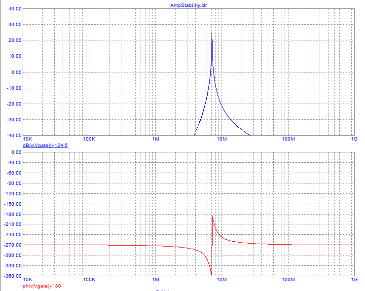
You
can see a huge resonance, which is to be expected in a tuned amplifier
with undamped input circuit. The phase of the feedback is -270° over
most of the frequency range, but touches -360° at the lower side of
resonance. At that frequency the loop gain is a little above 0dB, so we
have perfect conditions for oscillation.
Let's try to fix this
amplifier. First, I will add shunt feedback, with a 300Ω resistor. The
resonance broadens, and the phase response changes dramatically:
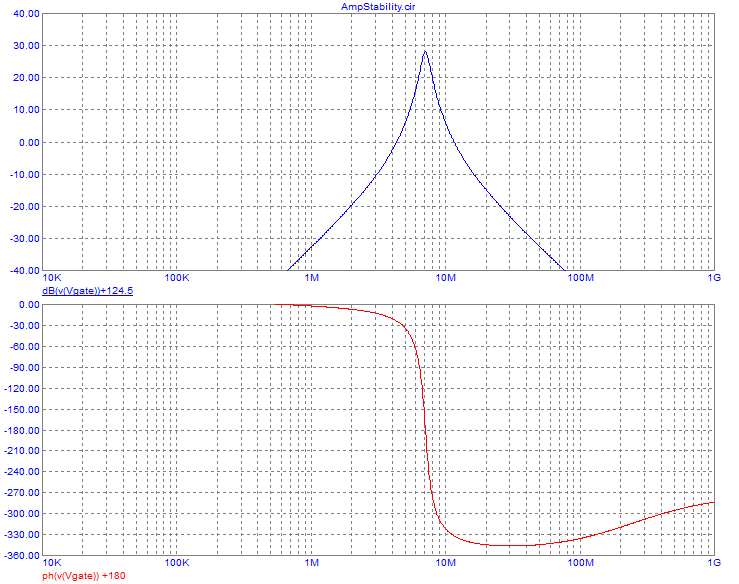
Why
this drastic difference in the phase plot? Well... Two resonant
circuits can cause twice as much phase shift as a single one. In the
previous example we had no resistors between the two resonant circuits,
so at the exact resonant frequency they were strongly coupled through
the drain-gate capacitance, acting as a single resonant circuit.
But now, with resistive feedback overwhelming the capacitive one, we
actually separated the two resonant circuits, getting twice as much
phase shift! I had to change the -180° addition for the
transistor's phase inversion to +180°, to bring the curve back into the
graph's range, because it had descended out of range!
Despite
the larger phase shift range, the situation is now much better. At the
frequency of maximum gain, the feedback is nicely centered on
-180°. The phase margin at both the lower and the upper gain
crossover frequencies is about 25°, not really good, but at least the
amplifier now wouldn't oscillate. It would just ring like crazy.
Adding
a drive source with an internal 50Ω helps a little, but not enough. And
anyway an amplifier should be inconditionally stable even if the input
is left open.
Then I drastically de-Q-ed the circuit, by
changing the output tank to 1µH and 450pF, and the input tank to 3µH
and 150pF. The drive source has 50Ω, the input matching link is 30% of
the turns of the main coil. The result is:
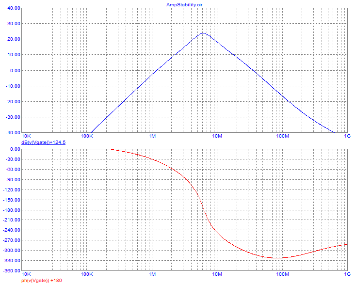
So
the resonance is much broader, the phase shift happens over a much
wider frequency range, the phase margin improved to 35° on the low side
and 47° on the high side. That's better, but still a little in the
ringing range. The conclusion is that tuned-input, tuned-output
amplifiers are always a little touchy, and it's a good idea to make the
loaded Q of any tuned circuits only as high as strictly necessary. This
also goes to the benefit of efficiency.
Many
times people run into trouble caused by resonant circuits they don't
even see. Consider this variation of out pet amplifier:
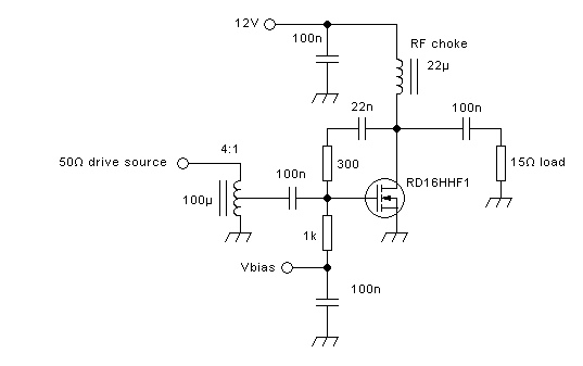
It's
a plain broadband amplifier with a 4:1 input transformer, simple
choke-capacitor output, a good shunt feedback to achieve good
linearity, stability, and flat frequency response, and even a bias
injection resistor doubling as gate swamping resistor at those
frequencies where the 100nF input coupling capacitor, and the 22nF
feedback capacitor, become ineffective. It should work fine, right?
Well, here is its feedback Bode plot, as usual without including any
delay caused by the transistor:
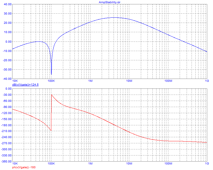
It's
pretty much as expected, except for the huge series resonance of the
input transformer with the 100nF coupling capacitor! That one causes a
sudden 180° phase shift, but it happens at a frequency where the loop
gain is already low enough, so it's OK. The phase margin is roughly
60°, which is actually fine. Note that below the resonant frequency the
gain rises just to 0dB again, but in that range the phase is fine. So this
circuit won't oscillate.
But what happens if the load is
disconnected? Hmmm... Let's see... No-load conditions are
always
risky, because then the transistor works into the choke's inductance,
adding a large phase shift to the feedback signal.
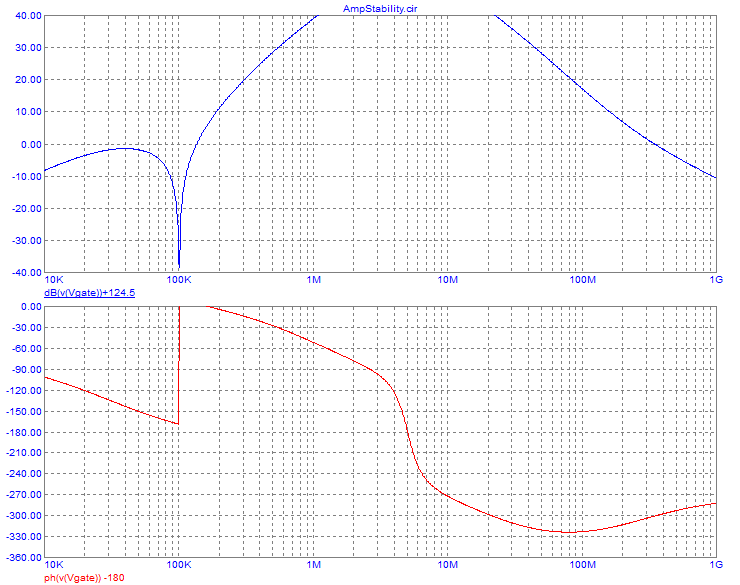
Yep,
we are in trouble! With the load removed, the phase of the feedback
crosses zero at a frequency where the loop gain is about 8dB. Our
amplifier will oscillate if the load is disconnected.
What can
we do to fix that? Well, we can use some damping of that series
resonance, by adding a resistor in series with that input coupling
capacitor. I chose 10Ω, just to try. The result is:
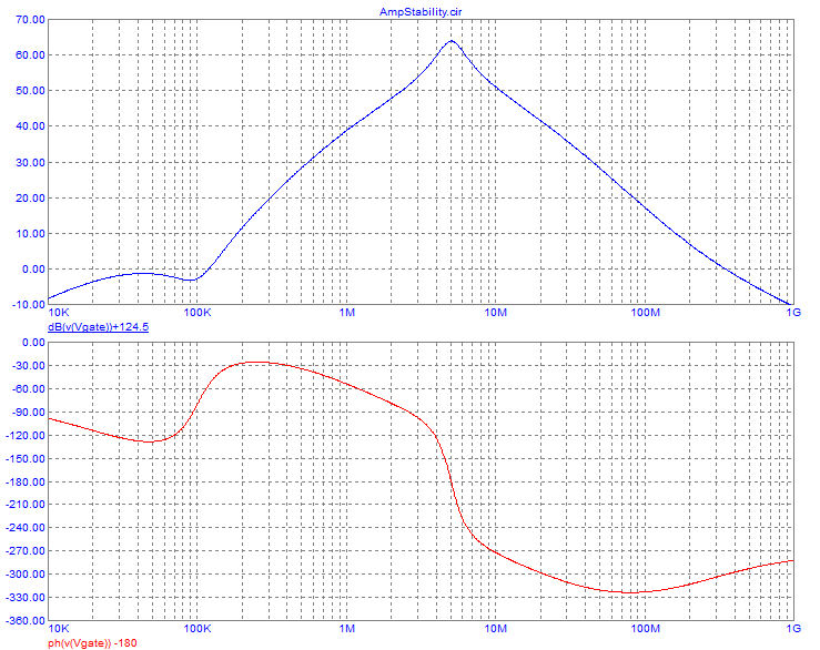
Well,
much better! The series resonance at 100kHz is now quite weak, and the
phase shift it causes is far less dramatic. The phase margin is still
not great, but good enough to avoid oscillation. Since we don't have
any drive in that very low frequency range, a tendency to ring down
there isn't too bad. But we definitely should always avoid any risk of
ringing inside the operating frequency range... And now look at the
area around 80MHz! There too the phase margin is a bit tight, while the
loop gain is still around 20dB. We need to watch what delay causes our
MOSFET, to make sure it doesn't cause trouble there, but
that's unlikely. We might end up with a poor phase margin at
30MHz,
and ringing, but remember, I'm analyzing the amplifier operating
without a load! It doesn't matter much if it works somewhat dirty, when
no load is connected. The important point is that it doesn't break into
potentially destructive oscillation.
By the way, the strong
resonance at 5MHz is caused by the feed choke resonating with the
transistor's output capacitance. Normally this resonance is very well
damped by the load, but when the load is gone, we see it.
So, our fixed circuit, tolerant of load disconnection, is this:
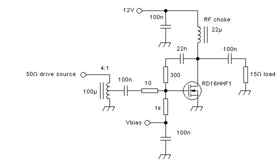
I
didn't check the input impedance matching now. Of course it's way off... A
good practical approach is to design a circuit including such a series
resistance in the input, calculating it for proper impedance matching,
and then simulate the loop to see if it will be stable.
Do
you like bad news? Stupid question, sure! But
whether or
not you like them, I need to tell you some: The above stability
analisis is extremely oversimplified, because I considered only a
single feedback path, the one inside the amplifier cell proper. A real
circuit will have additional feedback paths: Through the power supply,
through imperfect ground, through capacitive and inductive coupling
between components and connections, and through the source or emitter
lead inductance (very important)!
And in a transmitter we
rarely use a single amplifier stage just by itself.
The mixer
or DAC used to generate the transmit signal on the actual transmitting
frequency will typically deliver only about 1mW. But an HF transmitter
typically needs to produce anything between perhaps 10W and over 1kW
output power. So we need between 40 and over 60dB of gain, and that
can't be done in a single stage. So we get absolutely beautiful chances
to create a big, complex oscillator, due to the many feedback paths
available! Feedback inside each stage, over two stages, over three
stages, over all stages, even outside the amplifier block or whole
transmitter, by coupling between input and output cables, and so on.
Detecting, tracking down, understanding, and curing all those
instabilities provides never-ending entertainment, joy and fun to any
builder of RF power amplifiers.
Yes, I'm being sarcastic.
Oh,
I almost forgot: In any
push-pull stage of course you need
to understand, calculate or simulate the stability both for
differential mode and common mode. Even if the common mode isn't used
for amplification, it is present, and needs to be stable.
Let's
consider this 20W class AB amplifer:
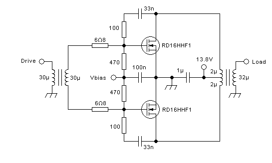
First
let's calculate its basics: The output transformer has a primary of 1
turn on each side, and a secondary of 4 turns. I will assume that
the
leakage inductance of the transformers is 1% of each winding, which is
pretty optimistic. When the load is 50Ω, the transistor that
is
conducting at any given instant sees a drain load of 3.1Ω in parallel
with 2µH, the feedback path, and its own output capacitance. On a good
day and with some luck, it might be able to pull down its drain to 2.5V
or so, given that the RDSon of these MOSFETs isn't brilliant, so we
have
roughly 11.5V peak amplitude, or 8.1V RMS at each drain, and 32.5V RMS
at the load, making a tad over 20W. Each transistor needs to conduct a
peak current of about 3.7A. The transfer curve up this page shows that
if we bias the amplifier to an idling current of 0.5A in each
transistor, we need to pull the gate about 2.5V peak above the bias
voltage. Since these 2.5V give us an 11.5V drain excursion, the voltage
gain from gate to drain is 4.6. The 100Ω shunt feedback resistor, which
sees 14V peaks, will conduct 0.14A peak, so at 2.5V peak on the gate it
loads the gate node with 17.9Ω. The 470Ω bias/swamp resistor lowers
this to 17.2Ω. The transistor's input capacitance has an effect at the
high end of the HF range, but not a big one. The 6.8Ω resistor
adds to the 17.2Ω to produce 24Ω load resistance on each side of
the drive trafo's secondary. The two sides in opposition then have a
drive
input impedance of 48Ω, plenty close enough to 50Ω to use a little
bifiliar-wound 1:1 balun as input transformer. 2.5V peak is required on
each gate, and due to the 6.8Ω resistors, forming a divider with the
17.2Ω gate node resistance, 3.5V peak is needed at each side of the
drive transformer secondary, making 7V peak total. That's very close to
5V RMS, and the same is needed on the primary side, thus this amplifier
requires a drive of 0.5W to produce an output of 20W. So its power gain
is
16dB. The low frequency limit is given by the mutual inductance of the
transformers, the high frequency limit is a combination of the
transformers, the transistors and the wiring, with the leakage
inductance of the transformers being the main limiting factor.
The
feedback path has a low frequency cutoff of 48kHz. It has to
be low enough to keep the feedback from phase-shifting at
frequencies that the transformers will pass well.
When
oscillations happen, they start with microscopic amplitude, so we can
do small-signal analysis for them. But they can start at any drive
level, and at any point of the driving waveform, so we need to do this
small-signal analysis not only at idling conditions, but also when a
transistor is conducting a high current. Since its transconductance
varies with drain current, stability conditions also vary. And since
the capacitances vary with voltage, that requires even more stability
analysis... Life isn't easy!
Let's make a first analysis in the
differential mode under zero-signal conditions, assuming an idling
current of 0.5A per side. Both transistors are on, and on the transfer
curve diagram we can see that the transconductance is about 0.8S. So,
by assuming a test signal injection of 1mV from gate to gate, one
transistor draws 0.4mA more, the other one 0.4mA less drain current.
For all analysis purposes they are in series, and so we can
draw
the following equivalent diagram for feedback loop analysis in a
circuit simulator:
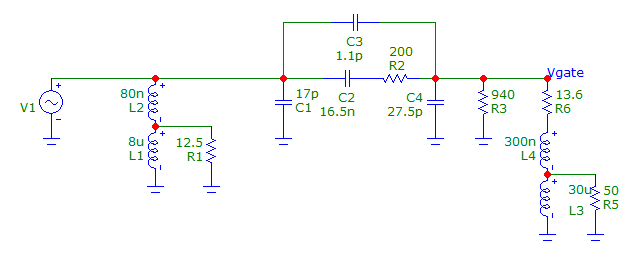
As
before, V1 is configured as a current source, injecting the calculated
drain current for 1mV between gates. L1 is the mutual inductance of the
output transformer, seen on its entire primary. Since each side of the
primary has 2µH, both in series and coupled
have 8µH. L2 is the leakage inductance of the output transformer. R1 is
the output load, transformed down, as it appears between drains. C1, C3
and C4 are the transistor capacitances, but expressed in pairs of two
in series. Likewise C2 and R2 is the shunt feedback, both in series. R3
is the two bias resistors in series, R6 is the two gate series
resistors in series, L4 is the drive trafo leakage inductance, L3 its
mutual inductance, and R5 is the internal resistance of the driving
source.
Under these optimal conditions, I get this Bode plot:
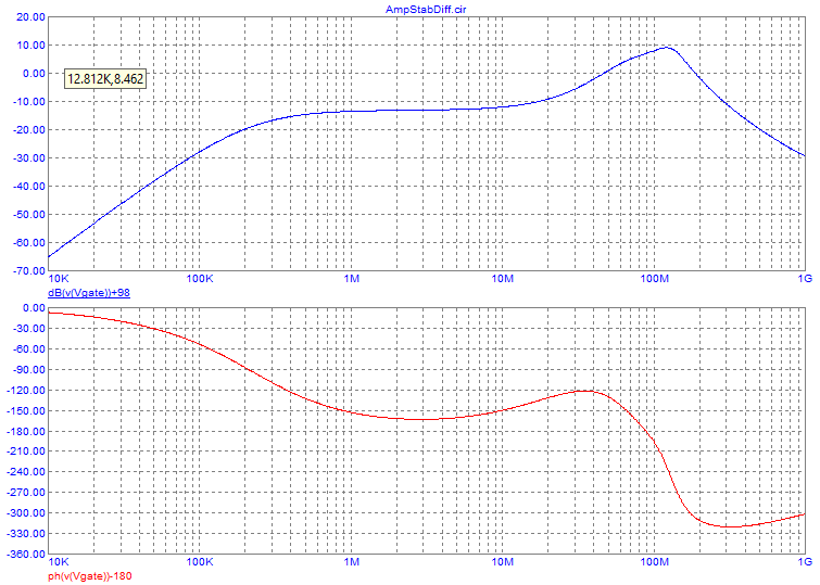
The
loop gain is very low. That's caused by the low MOSFET transconductance
at the bias current level, the low load resistance, and a considerable
dividing factor in the feedback network. The whole low frequency side
and the operating frequency range have no risk of oscillating, thanks
to the low loop gain. At the high side, the phase margin is about 50°,
good enough. Above 100MHz there is a peak in the loop gain, caused by
resonance between leakage inductances and transistor capacitances. The
fast phase shift in that frequency range is caused by this too, of
course.
Let's disconnect the load:
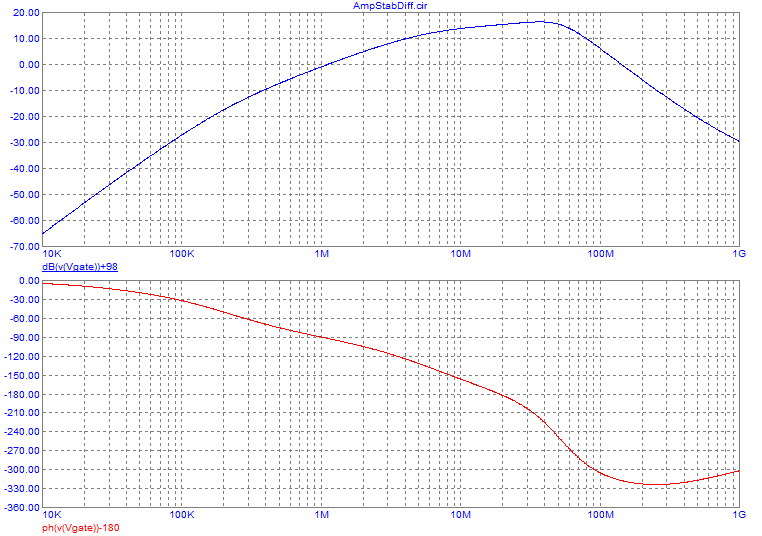
Now
there is much less attenuation in the drain circuit, so the loop gain
is higher to a lower frequency. Still the phase margin at the low gain
crossover is excellent, at 90°, while the one at the high frequency
gain crossover is only 40°, a bit small for comfort. If the
transistors add enough delay, we might see oscillation near
100MHz if the load is disconnected.
With a shorted output, we get this:
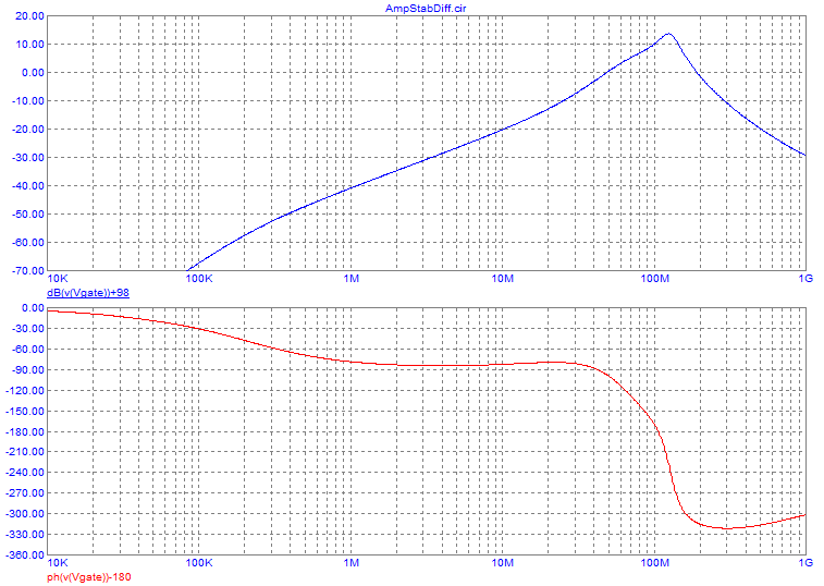
Again no problem at low frequencies, and a somewhat meager phase margin
a little below 200MHz, but it should be OK.
Removing
the drive source is fine, too. But then I tried to connect devilishly
chosen capacitive loads of 100pF to the output, and 26pF to
the
input. See what happens:
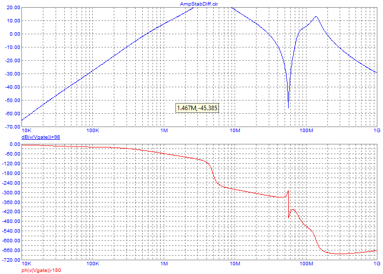
Note
that the phase scale had to be changed, to span two full revolutions! There is
a gain crossover at 30MHz with a phase margin of only 30°, too small
for comfort, and some pretty wild phase behavior that could lead to
further trouble when including the MOSFET delay. This behavior comes
from those capacitive terminations resonating with the transformers. It
probably wouldn't be impossible to make this amplifier oscillate, by
simply connecting short pieces of unterminated coax cable to the input
and the output, which can happen rather easily in practice. So, if you build such an amplifier, keep it decently loaded!
At least the -360° phase crossing happens at a frequency where the loop
gain is way down below 0dB.
When the amplifier is being driven at
full amplitude,
we have to look what happens at the instants when the drain
current is at about two thirds of the maximum value, which is
where the MOSFETs transconductance is largest. While at constant drain
voltage the transconductance reaches a peak at about 4A, it is lower
when at high current the drain voltage gets very low. That's why
amplifiers typically are most unstable near that two-thirds amplitude
point of the RF waveform. With a fast oscilloscope one can sometimes
observe little wiggles starting roughly there, which are VHF
oscillations mounted atop that part of the main HF waveform.
At
that time only one of the MOSFETs is conducting. Since I'm simulating
just the resistive and reactive elements of the circuit, not the MOSFET
transfer curve itself, the circuit used for simulation doesn't change.
Just the amplitude of my current source increases, because of the
higher transconductance. It is very close to 1.4S, so for 1mV between
gates, we have just 0.5mV on the gate of the active transistor, and
thus it's sinking 0.7mA on its side of the output transformer. But if
we keep the simulation schematic unchanged, we have to halve that
value, because the center-tapped primary acts as an
autotransformer/balun to put the voltage caused by that current on the
other side too, while the transformer acts as a 1:16 impedance
transformer, so that 3.1Ω load resistance appear across the transistor
that is on. We could change the diagram to reflect that, and then have
the current source inject 0.7mA, but the result will be the same. So
let's keep it simple.
In this case, it turns out that the
resulting 0.35mA of effective current injection into our
model is
even lower than the 0.4mA that happened when I analized the amplifier
at zero signal, with 0.5A idling current in each transistor. This is
rather unusual in practical amplifiers, and happened because I chose
0.5A idling current per side simply to start the current excursion
where the transfer curve begins its nearly straight part - but this is
really not the correct thing to do! For lowest distortion the idling
current should be selected so that the transconductance of each
transistor at the bias point is one half that at high current, and for this MOSFET that
would be at roughly 350mA or so per side. In that case the stability
analysis would give the same result at idle and at high drive. In
reality many people set the idling current of a class AB amplifier even
lower, looking for a compromise between linearity and efficiency, and
in that case the total transconductance of both transistors at idling
is lower than that of a single one at high drive, and then what I wrote
above is true: The amplifier has more risk to oscillate at strong drive
than when idling! Phew! My face has been saved...
Let's now look at the common-mode
stability. The equivalent circuit for feedback analisis changes a lot!
Because the transistors, working in equal phase, don't see the
load, which is applied only differentially through the transformer.
Also they don't see the mutual inductance of the output transformer,
because it's in opposite phase between sides, and thus cancels. But
they still see the leakage inductance between primary halves,
20nH. The two transistors act in parallel, so the
transconductance doubles, all the reactances and resistances are
halved, and so on. The input transformer simply disappears, since it's
balanced too, except that its interwinding capacitance might possibly
become important, so I will include it in the equivalent schematic. So
we end up with this:
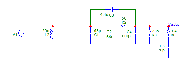
Always
keep in mind that such equivalent circuits are only coarse
approximations to the reality, which contains many unknowns. The
intention is to try to include all important bits and pieces, and very often this attempt is unsuccessful...
I
assumed 20pF interwinding capacitance for the input transformer.
Whether that comes close to the truth, depends on how it's made.
The Bode plot looks like this:
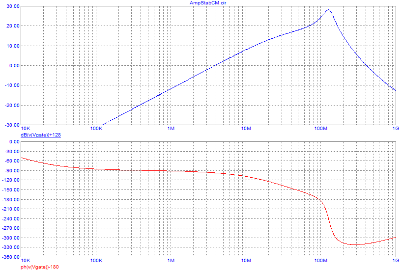
The
resonance of the output transformer's primary leakage inductance with
the transistors' output capacitance is obvious. The high side gain
transition occurs at 40° phase margin, but at a slightly lower
frequency there is only 35° phase margin, a bit tight, but it should do.
In the low frequency range the feedback has a phase close to -90°
instead of the desirable -180°, due to the fierce effect of the output
leakage inductance almost shorting the drain current, but still the
phase margin is excellent at the lower gain crossover frequency.
Disconnecting
or changing the load or drive won't have any effect on common-mode loop
gain, because the common-mode configuration just doesn't see those.
So it's all reasonably good, and this amplifer has a fair chance of
being sufficiently stable in all ways, for practical use!
Next
part of the "what if" game: What happens to the common-mode stability
if we change the feed configuration to two separate RF chokes? The
equivalent simulation circuit, is then the same, except that
we
get the full inductance of those chokes causing a rather high
common-mode drain signal voltage, from the drain current injected
there. The result is that the gain curve shifts up a lot, but stability
isn't compromised, because there is still about the same phase margin
at the gain zero crossings, due to the flatness of the phase response:
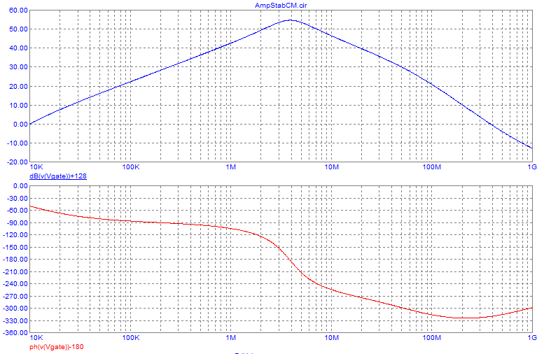
The point to watch is still the VHF range, where the transistors might
cause trouble due to their signal delay.
But
now let's do something evil. Some hams trying to build high power
amplifiers have done it, and have suffered the consequences! That evil
thing is removing the shunt feedback from such an amplifier that uses
separate RF chokes. This is what happens:
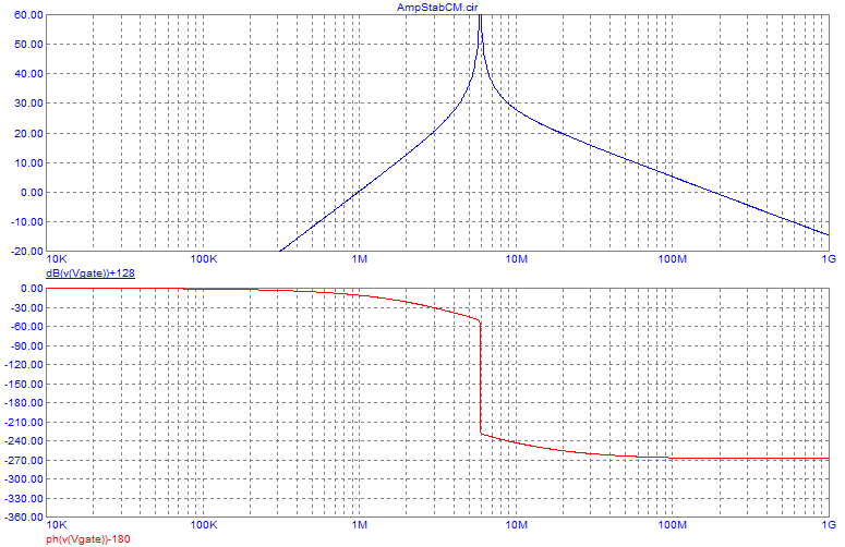
The
phase margin at the lower gain crossover is only a few degrees! Almost
certainly there will be enough strays in the circuit to move the phase
just a little further up, and we will end up with a 1MHz power
oscillator. And even in case it's so well built that there aren't
enough strays to give it that little phase boost, it will badly ring
when operating at 1.8MHz, with a phase margin of only 20° and a loop
gain of 10dB!
Such oscillation looks like both drains going down
and up together, and since the drain current can't go anywhere else than
into the relatively high inductance RF chokes, enormous drain voltage
spikes show up in each cycle of the oscillation, making the transistors
go full and heavy into avalanche conduction. Heavy enough to kill them
in an instant! There are hams who have killed a dozen or more high
power LDMOSFETs, costing over $200 each, due to this mistake!
In short: Common-mode oscillation due to lack of both common-mode feedback and
common-mode load.
Amplifiers that have coupled drains, through a
well-built bifiliar feed transformer, or a center-tapped output
transformer whose center tap actually works, are instead tolerant to
the lack of common-mode feedback. That's because only the leakage
inductance of the output transformer or feed transformer appears on the
drains in common mode, drastically reducing the common-mode loop gain,
and also preventing the appearance of those high inductive drain
voltage spikes. Of course at least differential-mode feedback should
still be used with them, to keep the gain, distortion, and frequency
response flatness under control, and the leakage inductance between
drains should be kept really, very, extremely low, making that point the priority #1 of the whole design!
There is also the nasty phenomenom of internal MOSFET instability.
Some MOSFETs will self-oscillate just by themselves, when they get the
right conditions. A MOSFET, after all, is a complex thing. In addition
to the MOSFET proper, it contains a parasitic diode, a parasitic BJT,
several resistances (which depend on temperature), several capacitances
(which are voltage-variable), several inductances, and in addition an RF
power MOSFET is composed of hundreds or thousands of tiny separate little
MOSFET cells! Be very careful when using a MOSFET outside of the
operating parameters recommended by the manufacturer. Crazily what
tends to make these MOSFETs oscillate is powering them from a lower
voltage than the nominal one, or driving them at a frequency below the lowest frequency
recommended by the manufacturer! For example, you might find a VHF/UHF
power MOSFET rated to operate from 1 to 500MHz, and another one rated for
100 to 500MHz. If you use the latter in an HF amplifier, it will
certainly amplify - but it might oscillate internally. And there might be no
way to stop this oscillation from the outside!
The best thing to do is to only use MOSFETs rated for a
frequency range that completely includes the intended one, and then
design a circuit with adequate phase margin. And when building
amplifiers that use a modulated supply voltage, make sure that you
arent' getting this kind of oscillation at the times of low supply voltage. Typically such oscillation is in the UHF range,
and appears only during a part of the main RF cycle. You need a good,
fast oscilloscope and test probe to see it. Sometimes such instability
can be cured by using more resistance in series with the gates, but in
other cases nothing works to fix it, and you have to choose a different
MOSFET.
Here are some suggestions
for building stable amplifiers:
-
Design the amplifier for just the gain you need. The more gain there
is, the more likely it will be unstable. The best way to reduce
excessive gain is through negative feedback, rather than using
attenuators.
- Keep the frequency response of the amplifier
limited to just the range you need. Coverage of any additional
frequency ranges is pointless, and increases the chances for instability.
-
In a multistage amplifier, let one stage, preferably the middle one, do
the strict bandwidth limitation, and keep the response of the other
stages wider. This avoids the situation where several stages contribute
phase shift on the same frequency, causing the overall phase response
to rotate through the oscillation boundary before the gain is down
enough. This technique is called dominant-pole compensation in some other areas
of electronics.
- Resistors are
my friends. Print this short sentence, frame it, and hang
it on the wall beside your workbench. If you want, add Never trust inductors
nor capacitors.
The reason for these two rules is that resistors don't cause phase
shift, while inductors and capacitors do. And phase shift makes the
difference between negative and positive feedback, and thus between a
stable amplifier, and, well, an oscillator. Every capacitor and every
inductor can cause up to 90° of phase shift. Keep their number small.
Swamp them with resistors, both in parallel and in series, wherever
necessary.
Even
a small amount of resistive damping will transform a
90° phase shift into a more moderate one, and very often this makes the
difference between a stable circuit and one that isn't. If you can
inject the bias through a resistor rather than an RF choke, use the
resistor. Make sure that MOSFET gates always connect only to
resistive paths. Specially avoid connecting any inductive element
directly to a MOSFET gate! A capacitor in series with the inductance
doesn't count. It has to be a resistor! And don't forget that chokes
and transformers are also inductors, nor that transformers have
invisible leakage inductors built in!
- Always
keep in mind that all bypass capacitors, coupling capacitors, RF
chokes, transformers, even if they have a reactance high or low enough to
be negligible over the entire operating frequency range, will
absolutely
have significant, phase-shift-causing reactances above or below that
range. Analyze their behavior essentially from DC to daylight, not just
over the intended operating frequency range.
- When physically
building an amplifier, keep the strays small. That means, make low
impedance interconnections extremely short and wide, to reduce stray
inductance. Make high impedance connections very thin, and keep them
clear of other stuff, to reduce stray capacitance. Analyze which
connections are most critical in this regard, and design the layout to
absolutely optimize them. A typical connection to keep extremely short
and wide is the emitter or source connection of RF power transistors
that operate at high current. That's why such RF power transistors have
two
to six emitter or source tabs, or use the mounting flange as
emitter or source connection.
-
Build amplifiers on a continuous ground plane. When using transistors
that use the mounting surface as source or emitter connection, solder
them to this ground plane. If you have to solder them to a heat
spreader, solder the underside of the board (used as ground plane) to
the heat spreader too, all around the transistor, to make a continuous ground plane.
-
Don't ever do the mistake that even some supposedly professional
designers love to do: Using several capacitors of different values in
parallel, for wide-range bypassing! It's nonsense, and it
doesn't
work, unless correctly done with a full understanding. It's
nonsense because even
pretty high value capacitors are physically small enough to have low
impedance up into VHF and beyond, and it doesn't work because when
connecting two different capacitors in parallel, the larger one starts
acting as an inductor at a frequency where the smaller one is still
capacitive, and you get a parallel resonant circuit that causes extremely poor
bypassing at the resonant frequency. The only case when such capacitor
paralleling works is when at least one of them is very lossy, causing
enough damping of the resonance they form. This could be the case when
paralleling a poor quality aluminium electrolytic capacitor, that has a
high ESR, with a
small SMD ceramic chip capacitor.
Instead paralleling identical bypass
capacitors, to provide a wider bypass path, or for current sharing, is
fine. But in most cases it's best to use a single
capacitor that is electrically large enough, and physically small
enough, to provide good bypassing over the whole frequency range
needed. Ceramic multilayer chip capacitors are pretty good for this.
-
When building several stages, arrange them linearly, rather than in a
circle or a compact blob. The output should be far away from the
input.
This
applies to connections and all RF parts, but even more so to the magnetics.
- Use proper shielding, at the proper places.
-
When using the same power supply for several stages, be very careful
with the decoupling. It should be effective over a wider frequency
range, both down and up, than the range over which the amplifier has
any gain.
- Watch for saturation of any magnetic cores used in
power supply chokes, and in other DC-carrying inductors and
transformers. Many people make mistakes in this area. The result is
adequate decoupling when there is no signal, degrading into
insufficient decoupling when the signal is strong and the DC is high,
resulting in oscillation that starts only above a certain drive level.
Very often such oscillation keeps going after the drive is removed,
because the oscillation makes the amplifier consume enough current to
keep the culprit in saturation.
- When building the final stage of a
transmitter, it's critically
important to understand and duly consider the effect of load impedance
on the phase and amplitude of the feedback.
That's because the impedance of an antenna, at the end of a
feedline, is totally unknown, usually quite complex,
and
totally different between one antenna and another. You could get
literally any load impedance on any frequency. So you need to analyze
your amplifier considering a drain load impedance that varies over the
whole range from totally capacitive to totally inductive, and from zero
to infinite magnitude. Now don't tell me that you are very careful with
your antennas, and they all have close to 1:1 SWR! That's only the case
on the few narrow bands for which they are built - but the
amplifier
sees them pretty much from VLF to somewhat above the cutoff frequency
of your lowpass filter! And the impedance in that range can be crazy.
Here is a Smith chart of my HF antenna's impedance, from 50kHz
to
30MHz. That's 4 dipoles, well separated, two of them having small capacitive loads, and fed through a roughly 30m
long 50Ω coax cable, giving low SWR on 80, 40, 20, 17, 15, 12, and 10
meters:
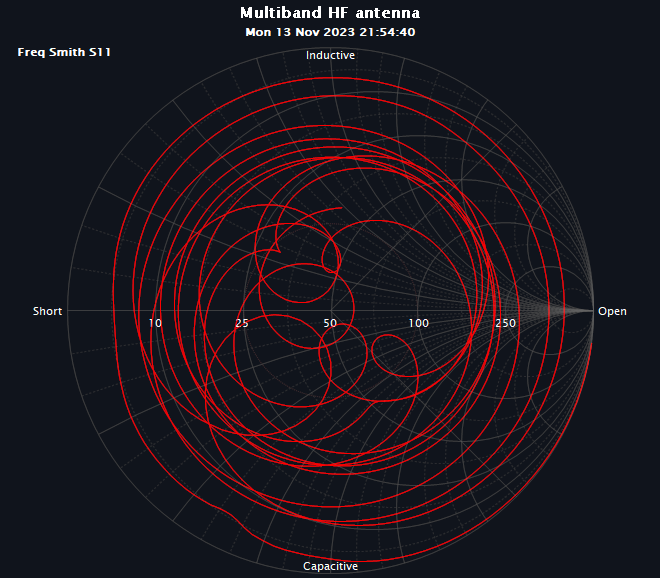
You
see? In the bands of interest, the impedance loops close
to the 50Ω center point of the graph, but outside those bands it goes in many circles between
open, almost shorted, very capacitive and very inductive. That's what
the final stage of a transmitter must handle, without becoming
unstable! The lowpass filter will change and complicate this impedance
further, the output transformer will modify it too, and so on.
I have to make a disclaimer:
I didn't double-check all my calculations and simulations about
stability. So there might be errors in them, even big errors. If you
find any, let me know. My intention was to show you a method of doing
stability analysis, rather than to give you practical, proven circuits
with accurate calculations. And there are other, better
methods
to do it, such as using the best simulation software you can find, with
exceptionally accurate non-linear transistor models that work even with
large signals and at RF, and then simulate the entire circuit,
including the transistors and all the many strays.
It's also
possible to build a circuit and test it, but with expensive RF power
transistors that's often a quite costly way, when you burn out a dozen
of them before you discover why they oscillate! And while an amplifier
that is definitely unstable will allow you to notice, in one way or
another, an amplifier that is just on the brink of getting unstable
might seem to perform well, only to start oscillating when conditons
change a little. Load impedance, temperature, supply voltage, bias
setting, drive level, whatever.
If you weren't already totally seasick from the many Bode plots, I
assume that the plot of my antenna's impedance definitely gave you the rest! So let's
end the chapter about stability. There is more to do.
Linearity
A sad thing in the life of anyone building linear amplifiers is that
transistors are fundamentally nonlinear devices. They introduce several
kinds of distortion, most of which can be broadly grouped into
amplitude distortion and phase distortion. Let's start with amplitude
distortion.
The transfer curve of a MOSFET theoretically follows a square
law. This can be seen very clearly in the data sheets of transistors
that haven't been optimized for linearity, but for efficient switching.
This is a typical example:
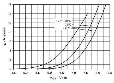
The parabolic shape of the curve is very obvious. But note that
the high temperature curve tends to straighten at
high currents, more than the curves for lower temperatures. This is
because the internal resistances of a MOSFET increase when hot, and
that causes the always- present source degeneration to become stronger.
Very generally, MOSFET transfer curves start with a parabolic shape at
low current, which bends into a relatively straight curve at high
currents, and does this more so at higher temperatures.
A manufacturer wishing to make a more linear MOSFET can do so by
deliberately increasing the internal source resistance. In this case
the parabolic section is much smaller, confined to the low current
zone, while from there up the MOSFET's transfer is relatively linear.
Such as in this example:
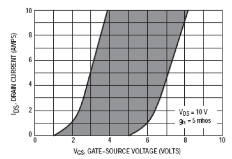
This graph shows a range, and the actual curve of the MOSFET will fall
somewhere inside, depending on temperature and tolerances. But you can
clearly see the response being exponential in the low current zone, and
pretty linear at high currents.
To get reasonably linear operation from a MOSFET like this in class AB,
you should bias it to a current that gives about half the
transconductance (curve steepness) as in the linear zone. In this
example, this would be about 1.2A. Due to their large nonlinear zone,
MOSFETs require relatively large idling current in class AB, if decent linearity is desired.
Biasing a transistor to the optimal point will still not result in
perfect linearity in the low current zone, but it's the best we can
do. If we want to build an amplifier that does not have this sort of
small-signal distortion, we need to build a class A amplifier, biasing
the transistor well into the linear range of the curve. That is, if we need
a linear drain current swing of ±3A, we need to bias this transistor to
at least 5A idling current! This would make a class A amplifier that
has pretty good amplitude linearity, at the cost of dismally poor
efficiency.
At very high current the transfer curve of a MOSFET the
transconductance will again get smaller, due to saturation effects. But
in linear amplifiers we hardly ever get into that range, because
usually the maximum power dissipation of the device limits us to lower
currents.
A MOSFETs drain current also depends to some extent on drain voltage.
This can be seen very well in a graph that shows drain current versus
drain voltage, for several gate voltages:
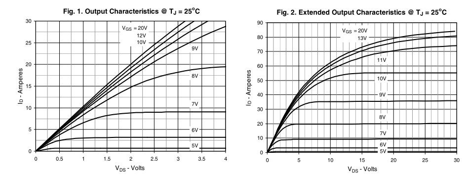
Here are two graphs showing the same thing, but the one at left is a
detail of the low drain voltage range, while the one at right shows the
curves for the same MOSFET over a higher drain voltage range. In the
right-side graph we can see that in the middle of the current range,
and at suffciently high drain voltages, the current depends only very
slightly on drain voltage. That is, the MOSFET is a very good current
source in that range, controlled by gate voltage. It has a very high
internal impedance, as all good current sources do. Instead at lower
drain voltages the curves bend. Operating a MOSFET in that zone causes
distortion. For example, if we used this MOSFET for a power amplifier,
operating at a peak drain current of 50A, we can see by interpolating
between curves that the transfer would start showing
saturation when the the drain voltage is down to about 11V. But this
same MOSFET can conduct the 50A with only 6.5V on the drain, if we
apply enough gate voltage! The gate voltage needs to be much higher,
though. So the ultimate waveform clipping of this amplifier would
happen at 6.5V on the drain, but driving it to go below 11V would cause
increasing distortion. In other words, we shouldn't drive it too close to saturation, if linear operation is desired.
Now this data is for a MOSFET that has a 250V maximum drain
voltage rating. Such a device would be used in an RF amplifier with a
supply voltage of about 80V. Avoiding distortion from flat-topping
(good old term!) requires us to sacrifice 11V of those 80V,
limiting the drain voltage swing to ±69V around the 80V supply. This
limits both the available clean output power, and the efficiency. If we
didn't care about linearity, we could run this MOSFET at ±73.5V,
getting a distorted sine wave of higher power and at higher efficiency,
or we could overdrive it like crazy to get a ±73.5V near-square-wave,
getting even more power and efficiency. This is fine with FM
transmitters, and with supply-modulated linear transmitters for AM or
SSB, but not for linear amplifiers.
In a graph showing such a family of curves, the basic linearity from
gate voltage to drain current can be seen by the separation between the
flat horizontal regions of each curve: They should be equally spaced,
for a reasonably linearized MOSFET. In curve pair above is for
a switching transistor with their typical square-law curve, which can
be seen by the spacing between the lower curves roughly doubling from
one interval to the next. Above about 60A this MOSFET enters the pretty
linear zone.
BJTs have a strongly exponential transfer curve, if you express it the
same way as for MOSFETs: Base voltage versus collector current. But
since the base voltage required to drive the collector over its whole
useful range is very small, it's typically more convenient to consider
the BJT to be a current-controlled current source. So we need to talk
about its current gain, hfe.
The hfe for DC, valid up to a certain pole frequency, is
usually given in the datasheets, but has an extremely wide tolerance.
The hfe at higher RF instead is given by the transistor's transition
frequency, Ft, also given in the datasheets, divided by the operating
frequency. Both values of hfe change with collector current, but not
nearly as much as the transconductance of a MOSFET. Here is
an example of the hfe at DC, for a typical BJT intended for
VHF amplifiers of a few watt output power:
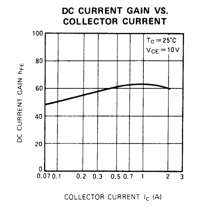
Only about 25% variation of the hfe, from a very small current right up
to the transistor's maximum rated current! This allows biasing BJT in
class AB to a very low idling current, and still get good linearity.
The RF hfe varies even less, seen here for an even smaller VHF BJT:
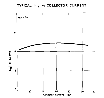
Even while the gain variation is much smaller than in a MOSFET, the
same basic pattern can be observed: Highest in the middle of the
current range, lower at both ends. But note how low the current gain
is. This transistor has a rated Ft of 1400MHz, so at 200MHz
its current gain averages about 7.
The family of curves that shows collector current versus collector
voltage, for different base currents, typically looks like this:
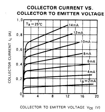
Comparing this graph to the MOSFET's, you can see that the curves are
quite evenly spaced, meaning good basic input-output linearity, and
also that the saturation level is much lower than for MOSFETs of the
same voltage rating, while also the knee, where the curves stop being
straight (linear), is lower. This allows driving a BJT's collector
closer to ground than a MOSFET's drain, allowing better amplifier
efficiency. This has to be taken with a grain of salt, though, because
the actual values depend on the exact transistor chosen, and there are
now mighty good MOSFETs available. Just when comparing transistors of
the same technology level, typically BJTs are both more linear and more
efficient, while MOSFETs have more power gain and much flatter
frequency response, giving them a progressive advantage towards higher
frequencies.
The curves for this BJT are not as horizontal as they are for the
MOSFET example I chose. This means that this BJT has a lower internal
output resistance, being a less good current source than the MOSFET example.
Since in RF power amplifiers we always have some shunt feedback,
intentional or not, that lowers the output impedance anyway, this
difference is irrelevant for RF amplifier use.
Phase distortion
is caused by transistors through several phenomena. One is that the
internal capacitances vary strongly with the instantaneous drain or
collector voltage. Varying capacitances in an RF circuit will cause
phase shifts. Here is an example of output capacitance for a typical
small BJT:
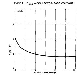
And here is an example for a typical small MOSFET, intended
for roughly the same frequency range, output power and supply
voltage as the BJT:
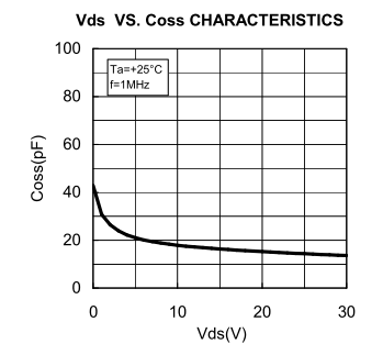
As you can see, the variation range is about the same for both, roughly
3:1, but the MOSFET's capacitance is about 10 times larger
than the BJTs! For this reason, MOSFETs generate much stronger phase
distortion than BJTs, and with MOSFETs it's much more important to
avoid driving them into onsetting saturation, when good linearity is
desired. The reason why MOSFETs have so much more capacitance is that
they work at a lower current density, so a larger silicon chip is
required to make a MOSFET for a given current. The good side
of this is that the MOSFET will then have a higher maximum
dissipation rating.
Another phenomenom that causes phase distortion is that the delay a
transistor adds to the signal tends to change with current, because the
Ft changes.
Memory distortion
is of a more special kind. The term refers to all those distortions
that depend on previous states of the amplifier. For example, thermal
effects depend on the instantaneous temperature of the silicon chip,
which is higher when the the amplitude of the signal is 70% after a modulation
peak, then when it is 70% before
that modulation peak. At both times the driving signal is identical,
but the transistor is still operating at a different condition, and
might amplify a little less or a little more. This distorts the signal.
Another way to produce memory distortion is to do what many designers
love to do: Plant an electrolytic capacitor across the supply line at
the amplifier. Typically the amplifier will be powered by a very well
regulated power supply, through a long wire. That wire causes voltage
drop. While the drive signal is getting stronger approaching a
modulation peak, the supply current increases, the voltage drop
increases too, but the capacitor will deliver some current, reducing
that drop. When the signal gets weaker after that modulation peak, the
current drawn is the same, but the capacitor is at a lower charge
state, is starting to recharge, and its voltage is lower than it
was before the modulation peak. So the transistors have slightly larger
capacitances, a little bit less gain, and we get distortion. It would
be better to either eliminate that electrolytic capacitor, or use an
extremely large one, or use very short and fat supply wires, or use a
power supply that supports remote sensing, and wire it up to regulate
the voltage at the amplifier, rather than at the supply.
Memory distortion effects tend to be rather small, anyway. They are
usually masked by basic amplitude and phase distortion. But when these
distortions are corrected for, memory distortion becomes measurable.
While the transistors are the main causes of distortion, some other
components can contribute some. Watch out for transformers and any
chokes or inductors that have magnetic cores and carry DC, because it's
rather easy to make a design mistake that results in saturation of the
core from DC. RF current will almost never be strong enough to cause
saturation, because the core will get extremely hot from
losses at an RF flux density very much below the saturation level. But
when a core gets somewhat into saturation due to DC, which happens
easily, the small RF current amplitude riding on top of this DC varies
the saturation degree of the core at the RF rate, causing severe
distortion. This is in addition to the other troubles caused
by saturation, such as a drastic drop in inductance.
Many kinds of capacitors vary their value according to voltage. This
isn't a big problem with bypass and coupling capacitors, because they
are usually chosen with adequate capacitances to cause very little RF
voltage drop across them, but any capacitors used in filters, resonant
circuits, for compensation or such must be of a type that is stable in
the presence of variable voltage. These are C0G ceramic capacitors,
called NP0 in olden times, porcelain capacitors, mica
capacitors, PTFE (teflon), the now-little-used polystyrene capacitors, and of course air dielectric and
vacuum capacitors. Some more probably exist. Just make sure that you
don't use any class 2 or worse ceramic capacitors in such places of the
circuit, such as X5R, X7R, Z5U, Y5V, X7S.
Also be careful with any diodes used in the RF area of the amplifier,
because these too have a voltage-variable capacitance when
reverse-biased, and a current-variable resistance when
forward-biased.
Resistors are our friends... Most of them behave pretty well. Just stay
away from carbon composition resistors. Modern film resistors
are much better. Old textbooks often recommend carbon composition
resistors for RF work, but that was simply because film resistors were
not yet available, and the only alternative would have been terribly
inductive wirewound resistors!
Negative feedback
reduces all distortions. But it's no magic bullet. It can only reduce
them a little, according to how much gain we sacrifice for that
purpose. A typical RF power amplifier will have a few dB
less distortion with negative feedback than without. People coming from
the audio world, using operational amplifiers having an open loop gain
of 120dB, to make an audio amplifier having 20dB gain, and using up the
excess 100dB gain in negative feedback to correct distortion, can
achieve a linearity that we RF guys can only dream about. But even if
what we can do with negative feedback might not seem like
much, it's definitely an improvement, so we should always make
good use of negative feedback.
Yes, it is possible to
correct distortion in a more complete way in RF amplifier
systems, and achieve an extreme degree of linearity. But we can't do
the trick of the audio guys, and use negative feedback spanning several
stages in a single loop. Given the phase delays in each of our stages,
such an approach is guaranteed to produce an oscillator instead of an
amplifier. What we need to do instead is more complex: Take a sample of
the amplifier's output signal, continuously compare it in amplitude and
phase to the drive signal, detect and "learn" the distortion curve of
each, updating it continuously, and then pre-distort the driving signal
in amplitude and phase, to make the nonlinear amplifier produce a clean output!
This can be done with analog circuitry, but it's complex and touchy.
It's better done with digital signal processing, and lends itself very
well for inclusion in software-defined radios. I use PowerSDR software
to play with this. Here is a graph of distortions and corrections of a
well-designed two-stage amplifier, using a single BJT driving a Gemini
LDMOSFET in push-pull:
In blue is the amplifier's amplitude transfer
curve, with the amplifer optimally biased into class AB, and driven
just to the onset of compression. You can see that the beginning of the
curve is very straight (linear crossover region), then bends a little up
to become steeper (higher gain in the mid-current area), then again
bends very slightly down (the very beginning of saturation).
In yellow is the phase response. It's normalized to the phase at full
power. You can see that between very small signals and full power,
there is about 5° of phase difference. This measurement was made at
7.1MHz, a pretty low frequency. The phase distortion gets larger at
higher frequencies, and smaller at lower ones.
The red and green curves are simply the correction functions needed for
predistorting the drive signal, to clean up these little residual
distortions of my amplifier.
The next curve shows the same amplifier, operated with much too low
bias, giving just 10mA of idling current:
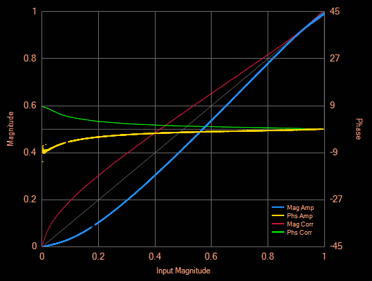
You can see the obvious, severe cross-over distortion. Basically the
amplitude response of the amplifier follows the MOSFET's gate-drain
transfer curve, slightly straightened by negative feedback. The phase
distortion is also higher, probably because at very low current the
MOSFET gets slower, causing more phase lag. That's why now the phase at
low power is 9° behind the phase at full power.
And the third graph shows the same amplifier, correctly biased, but
severely overdriven:
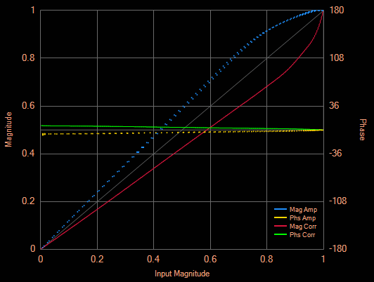
Never mind the dotted curves. I only made a brief test with a stable two-tone signal, collecting few
data points. What you see is a pretty linear amplitude response up to about
70% of full drive, then the amplifier goes progressively into
saturation. At full overdrive it's almost fully saturated, the output
power barely increases anymore with additional drive. There is also more phase
distortion (note the change of phase scale done by the software), with
the phase distortion making a slight bend in the saturation zone.
That's the internal MOSFET capacitances shooting through the roof as
the negative peak drain voltage gets very close to ground.
The beauty of adaptive predistortion is that I can run the amplifier
with moderately low bias, and overdrive it a little, getting higher
output power and much better efficiency, while at the same time
producing an exceptionally clean signal.
This version of the software cannot correct for memory distortion.
Doing so would require additional real-time computing. But thanks to a
stable supply voltage right at the amplifier, and very low temperature
variations due to this LDMOSFET having a huge dissipation rating
relative to the actual dissipated power, memory effects in this
amplifier are very low.
Such a distortion correction system samples the output signal only over
a specific bandwidth. In the case of PowerSDR, this is a little less
than 48kHz. Any distortion products falling outside that bandwidth
aren't "seen" by the software, and thus cannot be corrected. When the
software predistorts the drive signal to correct the signal inside the
bandwidth it sees, the distortion products outside that bandwidth
actually increase! For this reason it's important not to overdo the
overdriving and the bias reduction, to keep these far-away distortion
products small.
Of course whenever building or adjusting a linear amplifier, it's
essential to do proper distortion
measurement. If you check very old radio handbooks, you
will find several pages showing you photos of oscilloscope screens
displaying various patterns, usually created by feeding a dual
tone signal into the transmitter and watching the RF output. The book
author will try to teach you to visually recognize a signal having
various forms of distortion, such as flat-topping (saturation),
crossover distortion (incorrect bias setting), and others. Indeed this
was a good method for those times, particularly because vacuum tubes
don't cause the strong phase distortion of transistors, so the main kind
of distortion back in those years was amplitude distortion. Still,
measuring the intermodulation products on a spectrum analyzer is a much
better method. It will detect all usual forms of distortion,
and will accurately measure how much they impact the signal quality.
In ancient times, in the past millenium, spectrum analyzers were
excruciatingly expensive, and were to be found only in labs belonging
to rich companies. But nowadays a lot of very inexpensive spectrum
analyzers have become available. Their performance is typically not at
the level of a professional instrument, but plenty good enough to
measure the signal purity of transmitters. Tiny handheld ones exist,
also PC-based ones, and many digital scopes also have spectrum analysis
functions. If you buy any of these inexpensive things for amplifier
testing, make sure before you buy that it has enough frequency
resolution. To be really useful, it would be good if the resolution was
no worse than about 100Hz.
Here is an example of a spectral measurement done with PowerSDR, of my
little 60W amplifier, without predistortion, well clear of its
saturation, and with optimal bias setting:
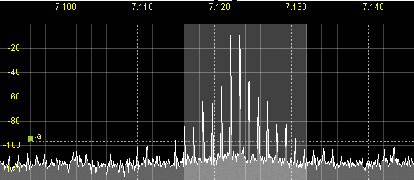
Never mind the red line, which indicates the suppressed carrier
frequency of my LSB signal, nor the gray bandwidth shown around it.
The two tones transmitted should appear nominally 6dB below the zero
line, because each contains one quarter of the peak envelope power, but
I drove the amplifier only to half power, so they are at -9dB
each. The next shorter lines are the two 3rd-order intermodulation
products. They are about 40dB below each tone, or 46dB below PEP. The
next two are the 5th-order products, 53dB or so below each tone. The
7th-order products are almost of the same strength, but the 9th-order
ones are much weaker, more than 70dB below each tone, making them
totally irrelevant.
Such a result is considered excellent signal quality, for
communications purposes. Most commercial radios are much worse than
this. But even this amplifier is very poor when compared to audio
amplifiers. Expressed in audio terms, the above spectrum would equate
to roughly 1.7% total distortion. A golden-eared HiFi fan would
break all olympic records while running away from such an
amplifier! Audio
guys shoot for distortion below 0.01% or so, and at least 90dB dynamic
range. In communications use, even 3% distortion and 40dB dynamic range
are considered to be quite good.
When varying the power, such a spectrum will not move up and down as a
block. Instead individual IMD product pairs will tend to rise more or
less, in various patterns. Typically a little into saturation the
5th-order products get as strong or even stronger than the 3rd-order
ones, and at even higher drive they fall back again. So it's never
enough when a manufacturer claims "3rd-order IMD is down by 40dB". He
should at least also tell how strong the 5th-order IMD was at that
power setting! Clever people love to play tricks here, turning the
power control for the lowest possible 3rd-order IMD, even if at that setting the
5th-order one is much higher! Specmanship at its best...
Time for a Blue Block, just in case...
Intermodulation
When any signal flows through any nonlinear device, distortion is
created. When several signals flow through that device, much more
distortion is created. Every signal (where one "signal" is a
single-frequency) mixes with each of the others, and with itself.
When signals mix, they create an infinite series of new frequencies:
All combinations of sums and differences between them. These are called
intermodulation products. How many signals or copies of the same
signals interact to create a new one, defines the order of the
intermodulation product.
A single signal going through a nonlinear device can only mix with
itself. For example a single 7100kHz signal will add to itself,
producing 14200kHz, this being a 2nd-order signal. This one
will again add to the original signal, creating 21300kHz, a 3rd-order
signal. The higher the order of a product, the lower is its amplitude.
These intermodulation products of a single signal with itself
are called the harmonics of that signal, because they are harmonically
related: 1:2, 1:3, 1:4, and so on. Interestingly there are cultural
differences in how they are counted: In English and Spanish we call the
2nd-order product the 2nd harmonic, the 3rd-order product the 3rd
harmonic, and so on, while Germans call the 2nd-order product the 1st
harmonic, the 3rd order product the 2nd harmonic, etc. Go figure...
I found this out the hard way. Don't ask.
The difference frequency between a single signal and itself is zero Hz,
that is, DC. This is the IMD view of why a diode creates DC from AC, when acting as detector
or rectifier. It's a way to see a simple process in a complex way...
Other difference signals between harmonics fall on the same frequencies
as other products, so there is no point in counting them separately.
When two different signals mix, matters get more complex. For example,
when mixing 7100kHz with 7101kHz, we get:
1st order: 7100 and 7101
2nd order: 1, 14200, 14201, 14202
3rd order: 7099, 7102, 21300, 21301, 21302, 21303
4th order: 2, 14199, 14203, 28400, 28401, 28402,
28403, 28404
And so on. The higher the order, the more products there are, and the weaker is each.
Note that even-order intermodulation products of nearby frequencies all fall far away from the
original frequencies, either at audio or into harmonic bands, while
odd-order intermodulation products fall both into harmonic bands and
into the operating band, very near to the original frequencies.
Audio products are easily suppressed by making an amplifier that
doesn't respond to audio. This is done using small enough coupling
capacitors, RF transformers with a not too low cutoff frequency, and
using RF chokes instead of wideband chokes. The products that
fall into harmonic bands are also easily filtered out by using a
lowpass filter after the last amplifier stage. A problem happens just with
those odd-order products that fall into the operating band. They cannot
be filtered out by any practical means, so if we want an amplifier that
doesn't cause severe splatter into neighboring channels, we need to make
it linear enough to suppress these products as much as required by the
application.
Thermal design
There
is just one way of killing RF power transistors that is even more
common than massive common-mode overvoltage spikes on the drains or
collectors: Simple, plain and old overheating! And in fact,
when transistors fail from overvoltage, this is typically also a case of
overheating. Just instead of overheating the whole silicon die,
typically just a small spot of it is overheated, through localized avalanching.
Hams and other
amateurs are particularly famous for overheating their transistors.
Don't get me wrong, I don't mean to imply anything negative in the word
"amateur"! After all, it means "lover". An electronics amateur is
someone who loves to do electronics, even if he may not be a
professional in the field. Such a person enjoys my deepest respect,
since I also started that way, at age 12, and I have very fond memories
of doing things with great enthusiasm, but without the faintest idea of how to do them.
There
are many rules of thumb which are simply not true, such as "If you can
keep your finger on it for 5 seconds without feeling pain, it's not too
hot." And a very common mistake made by amateurs is underestimating the
huge temperature gradient between a heatsink and the silicon chip inside a
transistor package. Many times when I told someone that he simply
cooked his transistor to death, I got the surprised statement "That
can't be the case, because the heatsink was barely lukewarm when the
amplifier failed." My standard reply to this is: "Well, what exactly burned out? The heatsink or the transistor?"
My point is that one
can easily end up with such a high thermal resistance between the
silicon die and the heatsink fins, that the heatsink stays stone cold
while the die dies from heat stroke.
The problem starts with the sad fact that most
amplifiers dissipate a lot of power. A simple old rule of thumb
(another one!) says that an amplifier will dissipate about as much
power in heat, as it puts into the antenna. Unfortunately this
rule falls very short of the truth, particularly for broadband linear
amplifiers used in SSB! Most such amplifiers end up working in
dynamic class A. They reach a peak efficiency, at full power, of
slightly under 50%, but their average efficiency over the whole
envelope waveform might be as poor as 20%. So, four times as much power goes
into the heatsink as into the antenna! Such RF amplifiers are really
room heaters with an auxiliary RF output!
Since hams, ship operators, and many other users of the HF bands only
operate sporadically, and transmit for very short times, efficiency
isn't important to most. But it's essential to make a proper thermal
design of such amplifiers, to keep the transistors alive over a long
time.
The essential points here are:
- Calculating the worst-case power that the transistor needs to dissipate,
- Deciding how hot we can allow the silicon to run,
- Finding out what our highest environmental temperature will be,
- Calculating the required thermal resistance from the transistor chip to the ambient, and
- Actually implementing the required low thermal resistance in our amplifier!
The
dissipated power varies a lot over the RF cycle, and also over the
envelope cycle. It also varies with load conditions. We don't need to
consider the variations over the RF cycle, because thermal inertia of
the silicon chip proper is plenty large enough to average the temperature of
the chip over a whole RF cycle, and even several cycles. But we do need
to consider the dissipation fluctuations over the envelope waveform,
and the easiest way to do that is to simply consider what will happen
at each particular drive level, when transmitting a plain carrier. The
highest dissipation will typically not happen at full power output, but
at some lower level. The exact power output that causes maximum power
dissipation varies with the bias level, amplifier type, and so on. If
we make sure that the silicon chip stays cool enough at the worst
possible drive level with a plain carrier, it will also be fine over
the whole envelope of an SSB signal.
Datasheets always state an
absolute maximum allowed junction temperature. Depending on transistor
characteristics, such as the metal used to contact the silicon, this
absolute maximum temperature may be anything from 150 to 225°C, for
silicon transistors. But this does not mean that we can operate a
transistor for a long time at the rated temperature! Instead its life
span will be short, if operated that hot. We need to keep it cooler if
we want it to last. How much cooler, depends on how long a life we
want it to have, also on current density in the silicon, and other things.
Manufacturers often provide information relating chip temperature to mean
time before failure, for specific operating conditions, specially
current. These can be used if available. Otherwise, as a rule of thumb
for typical intermittent use by hams and similar users, running a
transistor about 30°C cooler than the absolute maximum rated
temperature usually results in an acceptable life span. But if
high reliability is desired, the temperature should be kept even lower
than that. Keeping a silicon chip below 100°C results in unlimited life
span, on a human time scale.
Ambient temperature depends on
where the equipment will operate. When using it in a fresh climate, or
in air-conditioned rooms, and the heatsink is located outside the radio
in free unconfined air, 25°C is a good value to take. But in most cases
we have no assurance that a radio will always be used under such benign
conditions. Depending on the situation, we might need to assume a
maximum ambient temperature of 35°C or even more. And if the heatsink
is inside the radio, or enclosed in any other way, we need to carefully
evaluate how high the air temperature in that space might get.
Once
we have the maximum actual dissipated power, the maximum junction
temperature that will give a good life span, and the maximum ambient
temperature, it's trivial to calculate the total junction-to-ambient
thermal resistance needed.
Achieving it is a totally different
matter, and is the hardest part of the process. Transistors normally
come with their internal junction-to-case thermal resistance clearly
specified, but from there on we are on our own. The total thermal path
of a typical transistor mounted on a heatsink is a series connection of
these:
- Junction to case
- Case to heatsink
- Inside heatsink
- Heatsink to air
Junction-to-case
thermal resistance is known, but the others usually aren't. The
case-to-heatsink thermal resistance is dramatically dependent on the
mounting method: Soldering the transistor to a smooth heatsink surface
is good. Bolting it down with a very thin layer of good heat-conductive
paste is bad. With a
less good paste, or a thicker layer, it's even worse. Dry mounting,
without any paste or other filler, is horrible. And any sort of
insulated mounting, be it with mica, ceramic, kapton, silpad, is worse
than horrible. Silpad mounting is about as bad as mica installed with
heat conducting paste on both sides. In all these cases, clamping is
often better than bolting, and smooth flat surfaces are better than
rough, irregular ones.
I don't mean that insulated mounting, thermal grease, bolts and
clamps, can't be used. They do have their place, because in a great
many situations their performance is good enough. But when you need the
best thermal performance, there is no alternative to soldering the
transistor to the heatsink.
The
thermal resistance inside the heatsink is the worst-understood item of
all these. The transistor might have a mounting surface of only 1
to 4cm². But the heatsink is large. The heat has to travel from
the transistor mounting spot to every last corner of the last fin. Some
paths are short, like a few millimeters from the mounting spot straight
through the base plate to the closest spot where air touches. And some
paths are long, like 20cm from the transistor mounting spot to the
corner of the farthest fin of a moderately large heatsink. In between there are
infinite other path lengths, and they have varying cross sections.
Calculating this precisely requires relatively advanced maths, so many
electronicians will instead prefer to use simplified calculations,
approximating the final value by dividing the heatsink into just a few
sections for calculation, or use online thermal calculators to get the
job done. The all-important point here is to never forget the thermal
resistance of the spot under the transistor, and in the lateral conduction inside the heatsink's base plate! Too
many people forget to consider them, and their transistors overheat.
When
using a commercially made heatsink, the heatsink-to-air thermal
resistance is usually given by the manufacturer. But there are two big
catches, and a small one. The first big one is that this value is valid
only for very specific conditions, such as free natural convection with
a specific temperature difference, or perhaps it's rated for a given
airflow rate, using a specific fan. When using natural
convection, the heatsink-to-air thermal resistance varies dramatically
with heatsink temperature, because a hotter heatsink causes much
stronger convection. So a very nonlinear ratio results between
dissipated power and heatsink temperature. With a small power it
already heats up a lot, but with higher power the additional heating is
progressively smaller. It also varies a lot with the orientation of the
heatsink. Vertical fins, with free access from below and above, is
best. When using a fan, or some other form of forced convection, the
heatsink-to-air thermal resistance becomes much lower, and almost independent from the
dissipated power and orientation.
The second big catch is that when a manufacturer specifies the thermal
resistance of a typical heatsink consisting of a flat base plate with fins
on one side, he assumes that the heat source will be evenly distributed
over the entire flat surface of the base plate! But this is very rarely
the case with RF power amplifiers, and so the actual thermal resistance
from the transistor's mounting spot to the air is higher, and often
very much higher.
Finally, the small catch is that this rating is only valid at sea
level. As soon as you use the radio in a higher location, the air is
thinner, so the heatsink-to-air thermal resistance gets worse. You
either need to recalculate it for the altitude at which you will
operate the equipment, or for the highest altitude at which someone may
want to operate it. And that's why most equipment has a maximum
operating altitude specification!
When designing an amplifier, you need to be specially aware of thermal bottlenecks,
where a lot of heat flow concentrates. It's most important to keep
thermal resistance low at those places. The heat is all generated in a
tiny silicon chip, and silicon is a relatively poor thermal conductor,
so there we have the most important bottleneck. Then the heat spreads
out a little in the transistor's metal base, and that's the second
bottleneck. Both of them are added up and specified by the manufacturer
as the junction-to-case thermal resistance. We can't change
the insides of an existing transistor, but we can select a
transistor that is adequate for our needs. And if none exists, we can
combine two or more transistors, which results in a lower total internal
thermal resistance, since they are thermally in parallel.
The
next bottleneck is the case-to-heatsink interface. This one is under
our complete control, and we need to make its thermal resistance low
enough. This is done by avoiding insulated mounting when so required
for low enough thermal resistance, using good thermal paste if needed,
and soldering the transistor to the surface when even better
performance is needed. The ratio between the thermal resistance of an
insulated mounting, and that of a soldered one, can easily be as much
as 100:1! And the other important thing is using a
material under the transistor that has good enough thermal
conductivity. Most heatsinks are made from some aluminium alloy, that
has worse thermal conductivity than pure aluminium, and much worse than
copper. That's why in demanding situations a copper heat spreader is
used between the transistor and the heatsink. Its main benefit is
reducing the thermal resistance in that thermal bottleneck right
under the transistor, but an added benefit is improving the lateral
thermal conduction along the heatsink's base plate. Its downsides are
lengthening the thermal path from the transistor to the air, and adding
an additional interface layer, between the spreader and the heatsink,
which is usually only bolted and greased, but can be made large enough
to have low thermal resistance anyway.
Since the thermal
calculations are rather complex, I use online thermal calculators to do
them. I prefer not giving links here, because such web pages come and
go. Just search for some, and try them. It takes some time
understanding them and learning to use them properly.
Water cooling
is attractive when a large amount of heat has to be removed. Since
water has an extremely large thermal capacity, only a small flow rate
is needed, and this small amount of water needs only narrow channels,
so it can be passed extremely close to the transistor, by using a
properly designed cooling block. A small copper block with many very
fine water channels in it, fed with pressurized water, is most
effective. The flow will be highly turbulent, producing low
copper-to-water thermal resistance, and the fine structure allows
having a large transfer surface very close to the transistor,
minimizing the thermal path length through copper.
Many
people
instead use a large copper block with fat water pipes or channels in
it. This tends to still be better than air cooling, but not nearly as
good as a micromachined small cooling block. Those large blocks are
best for distributed heat sources, like some large modules often used
in industrial power electronics.
The
water
can either be cooled back down in a radiator, with or without a fan, or
for intermittent, low duty cycle use, it can simply be kept in a large
enough container, mostly just storing the heat while the amplifer is
used, and
releasing it slowly and continuously through the walls. For normal ham
operation at the legal limit power, a 20 liter cannister under the desk
is
usually sufficient. With such a system the only noise of the cooling
system is the pump, and if an immersion pump is used it can be
inaudible.
Protection
Brave people don't include protection circuitry in their amplifiers.
They try to always use the correct antenna, make sure that no
connectors are loose, badly soldered, and that no bird ever sits on the
antenna while transmitting. Sometimes they are lucky for a long time,
but eventually Murphy gets them.
People aware of Murphy's Laws
add several levels of protections, and then some. But Murphy still gets
them, by making some protection misbehave in a way that kills the
amplifier while shutting it down, or whatever.
When you build an
amplifier, only you can decide if you want protections, and which ones.
In case you are of the brave kind, skip this section!
The
problem is that almost all higher power amplifiers can be destroyed by
incorrect loading of some sort. Not all bad load conditions will
destroy a given amplifier, but some may. Some amplifier might survive a
shorted load but burn out when left open, or the other way around. Some
amplifier might burn out with any excessively inductive load but
survive all capacitive ones, or the other way around. And many
broadband amplifiers will be susceptible to dying on one condition on
one band, and a totally different condition on another band! That has
to do with phase shifts inside the circuitry, which are totally
different according to frequency.
Other conditions that can kill amplifiers are excessive temperature,
overvoltage at the supply, reverse polarity, overdrive, driving at a
frequency outside its range, leaving the input open, nearby lightning,
not to mention water ingress, condensation, snails, spiders and other assorted critters making a home inside, etc.
Many people use
SWR sensing circuits, that reduce the drive power or even shut if off
when the SWR exceeds a certain level. Such a protection can indeed save
an amplifier from many mishaps, but it needs to be fast enough. Many
aren't. Transistors can take huge overloads of some kinds, but only for
a very brief time, microseconds to milliseconds. To save a transistor,
the protection must react within this time.
An
SWR sensor placed
between the low pass filter and the antenna output will not protect
against accidentally switching in the wrong filter, or transmitting on
a frequency above the cutoff of the selected filter, or a relay
failure, which are common. If instead the sensor is placed right
after the amplifier block, before the low pass filters, it will
protect
against that, but the protection might trigger on the normal reflection
of harmonics from the filter. Depending on the amplifier type
(producing more or less harmonic output), a decision needs to be made.
Some amplifiers even use two SWR sensors, one before and one after the
filters, the first one being less sensitive than the second one.
Any
condition that causes higher dissipation than the maximum one assumed
in the thermal design, can make a transistor burn out. To effectively
protect against this, a protection circuit needs to continuously
calculate the actual dissipated power. This can be done by sensing the
supply voltage, supply current, forward power and reflected power, and
then making the calculation:
Dissipated power = voltage × current + reflected power - forward power
It's
easiest to make these calculations in a microcontroller. It needs to be
fast enough. How fast it needs to be, requires a transient thermal
resistance calculation, using data provided in the transistor's
datasheet. If a microcontroller turns out to be too slow, analog
multipliers and op amps can be used instead. They are fast, but analog
multipliers tend to be somewhat expensive.
Such a circuit will
protect against many accidents. Particularly it can protect against
lowpass filter switching errors and relay failures, without requiring a
sensor between the amplifier and the filters. It can also avoid many cases of destruction from self-oscillation. But it
does not provide sufficient protection from conditions that
cause abnormally high drain voltage peaks, because those make a
transistor go into avalanche conduction, and the power dissipation capability of a
transistor during avalanche conduction is much lower than during normal
conditions, because the avalanching tends to happen in a very small
area of the silicon chip, concentrating all the heat there.
So
it's a very good idea to add direct drain overvoltage protection. It's
a circuit that takes a sample of the drain voltage, on both sides for a
push-pull amplifier, detects the peak voltage, and acts very quickly if
this gets dangerously close to the absolute maximum rated voltage of
the transistor.
Another protection that is good to have is fast-acting overcurrent protection in the power supply.
A
builder has to decide what to do when a protection circuit detects a
dangerous condition. Reducing the drive power is effective in some
cases, but not in others, such as those brought on by self-oscillation.
Completely cutting off the drive is not much better. Shutting down
the power
supply is very effective, but tends to have some delay due to charged
electrolytic capacitors. If the delay is too long, an additional MOSFET
switch has to be added after those capacitors, instead of shutting down
the power supply through its control circuit. Reducing or
shutting off the bias isn't a very good protection method for
LDMOSFETs, because they are not very tolerant of negative gate voltage.
If the bias is turned off but drive is kept on, gate damage might
result, killing the LDMOSFETs, particularly if ALC is used, that reacts
to the sudden drop in output power by increasing the drive! In any
case, if protection is
implemented via bias shutdown, the bias voltage needs to go down slow
enough to avoid causing a drain voltage spike by induction in any
chokes
present in the supply path. Such a spike can make a bad situation
worse, by momentarily adding to the avalanche conduction!
Complete
shutdown of the amplifier in the event of an abnormal condition is
better than drive reduction. Of course it results in an interrupted
transmission, but it may save the amplifier! The protection circuitry
should clearly display the reason of the shutdown, until the operator
resets it, because having to make the protection shut down the
amplifier over and over, to find out the reason, is extremely risky.
Perfect,
foolproof protection doesn't exist. Add that to your list of rules.
Fools are foolish enough to kill any amplifier. But one can drastically
reduce the risk for normal people killing amplifiers, by using good
protection circuits.
Don't believe false advertising!!!
A video has been circulating for years, in which a company
pretends to demonstrate that one of their high power LDMOSFETs is
indestructible. The video shows a test setup with power supply, drive
source, power meter, load, and the operator disconnects the load,
shorts the amplifier's output, drawing very pretty sparks, while the
amplifier survives unharmed. But the video totally fails to mention
that the amplifier is being driven by a pulsed signal, at a low
duty cycle! The RF power meter is a peak-reading one, so at first glance it
looks like a continuous RF signal is used. Not so! By paying attention
to the power supply displays, it's clear that the amplifier is
operating at a low duty cycle.
Also the datasheet of that
transistor, and many others, claim that it will survive very high or
infinite SWR at all phase angles. Again, that's only true under
the operating conditions of the test circuit shown, with excellent
cooling, and with the low duty cycle specified in the fine print.
In a typical broadband circuit, in SSB, let alone RTTY, and
realistic/practical dissipation conditions, these transistors will
definitely not survive that high SWR at all phase angles!
You have reached
The End
Phew!
This article took barely four years to complete.
Back to homo ludens
electronicus.