50W LDMOSFET HF
linear amplifier for the Red Pitaya
 Almost
four years ago, in early 2017, I decided to get into software-defined
radio, and for that purpose I bought a Red Pitaya board. The main
project
is a transceiver that has a high efficiency, legal-limit output stage
employing envelope elimination and restoration. I started doing the
development work, but I found rather little interest in such a
project among fellow hams. Some even ridiculed me for striving towards
highest possible efficiency, arguing that energy is cheap enough that
it's no problem to waste some. These reactions, along with the general
state of ham radio, which I perceive as being in serious decadence, damped my
motivation. I got lazy, and the project has been resting in a state of
half development for years.
Almost
four years ago, in early 2017, I decided to get into software-defined
radio, and for that purpose I bought a Red Pitaya board. The main
project
is a transceiver that has a high efficiency, legal-limit output stage
employing envelope elimination and restoration. I started doing the
development work, but I found rather little interest in such a
project among fellow hams. Some even ridiculed me for striving towards
highest possible efficiency, arguing that energy is cheap enough that
it's no problem to waste some. These reactions, along with the general
state of ham radio, which I perceive as being in serious decadence, damped my
motivation. I got lazy, and the project has been resting in a state of
half development for years.
But I did a lot of listening with the Red Pitaya and PowerSDR software,
which provides very much better performance and functionality than my
old conventional Kenwood transceiver. Only for transmitting I went
back to the Kenwood. Eventually the idea matured to build a little
amplifier that would allow me to put the Red Pitaya on the air, in a
basic way, with a usable power, although without the cost of a high
power amplifier nor the complexity of EER.
I had purchased a small, inexpensive, 70W-rated gemini LDMOSFET, intending to
use it as an expendable guinea pig in a scale model of the big
project's legal-limit class D final amplifier. So I decided to use this
device to build a provisional small amplifier for the Red Pitaya, laid
out in such a way that it can still be used for experimentation towards
the big project. Since the small, 13.8V-fed amplifier works with the
same drain load impedance as a big 50V-fed one, such experimentation is
quite realistic.
This little amplifier is an attempt at operation in totally, absolutely
conventional class AB, unlike most HF broadband push-pull amplifiers,
which are mixed-class designs, operating somewhere in the continuum
between class AB and current-switching class D. The idea was to provide as much signal
quality and efficiency as class AB can deliver. How much success I had
in this attempt will be shown further down this page, in the section
about test results.
The Red Pitaya delivers a maximum output power of
10mW, and
it's best to run it a few dB below its maximum output, so a 50W
amplifier needs to have about 40 to 42dB gain. While LDMOSFETs
are capable of very high gain at HF, 40dB is a little high. So I
decided to build a two-stage amplifier, and divide the gain roughly
equally between the two stages.
To keep the circuit simple, I wanted to use a single-ended class A
driver stage. I experimented with various FETs, but found that these
are simply too non-linear to use in single-ended circuits. It would be
necessary to bias them to a comparatively very high standing current in
order to get good linearity. BJTs are very much better in this regard,
being far more linear than FETs over a wide range of collector current,
thus allowing to bias them just high enough to avoid clipping on signal
peaks. Unfortunately production of RF power BJTs has essentially been
discontinued. But I have some in my junk box. I selected a very
antique but excellent 2N5109, fully knowing that the use of a
discontinued device won't be very popular with people who want to copy
my design but don't have such an animal in their junk boxes. Sorry... I
just used what I had!
The final stage is built around a modern LDMOSFET, an AFT05MP075N. This
device is intended for VHF and UHF final stages in mobile radios, and
is quite inexpensive. I ordered it from a Chinese provider, but it's also
available at several of the well-known mainstream parts suppliers.
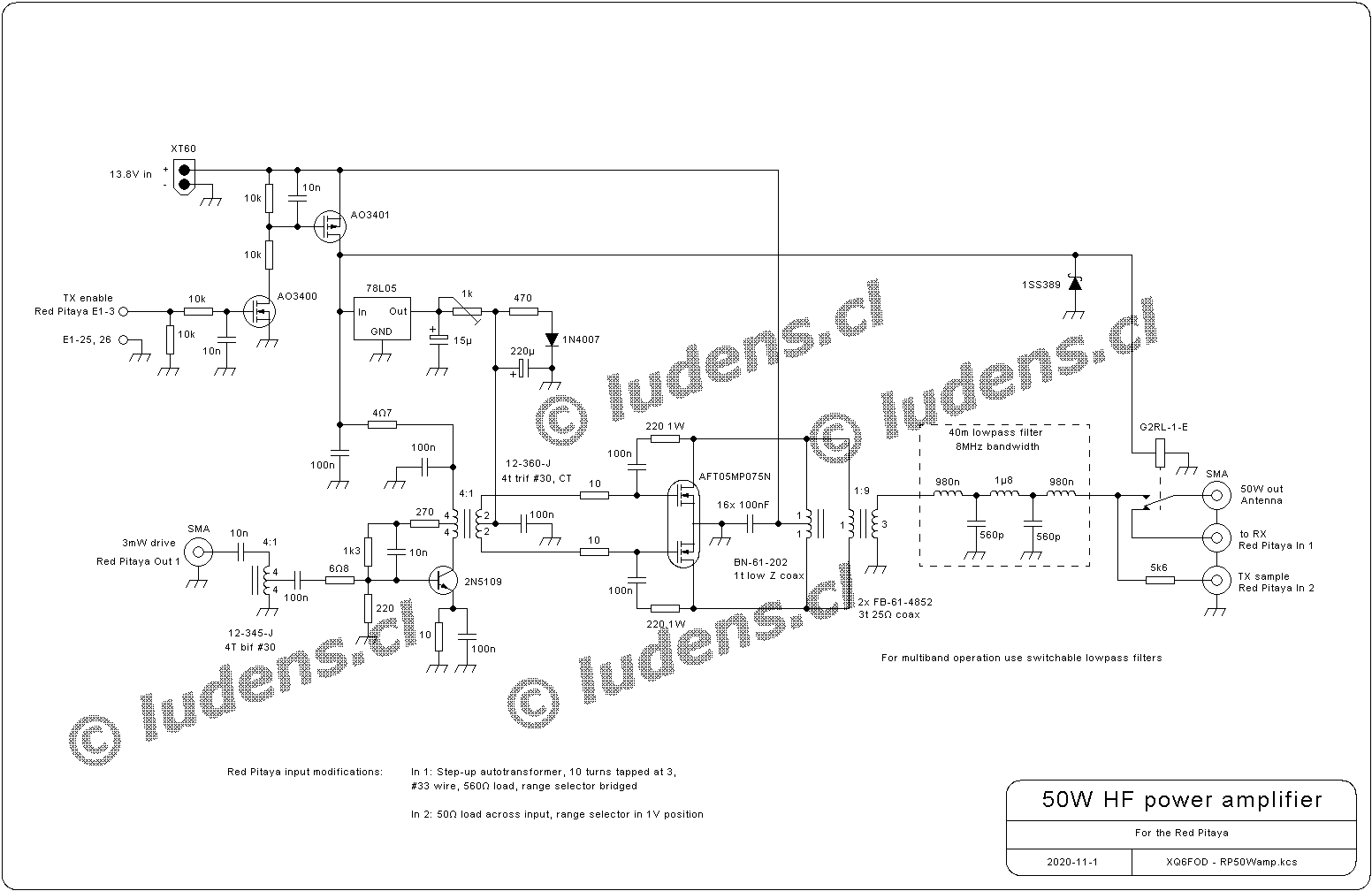
Without more ado, let's divide and conquer the schematic. You can get
the undivided and unconquered version by clicking on any of the parts.
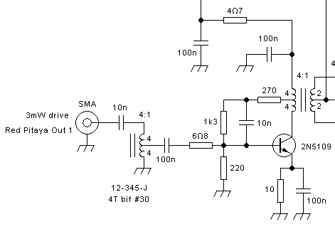 The
driver stage uses strong collector-to-base feedback and no emitter
degeneration, to achieve stability and good linearity along with high
gain. The feedback pickup point is tapped down on the output
transformer in order to improve the stage's efficiency by
wasting less of its available RF output power in the feedback
circuit.
The
driver stage uses strong collector-to-base feedback and no emitter
degeneration, to achieve stability and good linearity along with high
gain. The feedback pickup point is tapped down on the output
transformer in order to improve the stage's efficiency by
wasting less of its available RF output power in the feedback
circuit.
Due to the lack of emitter degeneration, presence of negative feedback,
and the high gain of this transistor, which has a transition frequency
in excess of 1GHz, the base input impedance is very low, behaving quite
a lot like a constant-voltage current node. To get
enough
drive current the Red Pitaya's 50Ω output is transformed down in a 4:1
autotransformer, and a 6.8Ω resistor provides the missing resistance
between the stage's low input impedance and the 12.5Ω expected by the
transformer. This resistor also serves to isolate the transistor from
the Red Pitaya's output lowpass filter, to prevent any instability.
Actually the design value for this resistor was 8.2Ω. I used 6.8Ω
because I had no 8.2Ω SMD resistor in my junk box... If you have one,
use it, to get the stage's input impedance closer to 50Ω. But don't use a 10Ω resistor, as it would be
too high.
As is traditional in this sort of amplifier stage, the standing current
is controlled by the base voltage, defined mainly by the three
resistors biasing it, the supply voltage, and the resistor placed at
the emitter. It's approximately 77mA. The ease with which one can obtain a sufficiently stable bias current in a
simple circuit, without a need for adjustment, is one of the advantages
of BJTs over MOSFETs.
The input transformer is wound as four bifiliar turns of AWG #30
enameled wire twisted together using a drill, on a small Ferronics
12-345-J two-hole ferrite core. A suitable replacement for this core
would be an Amidon BN-43-2402.
The interstage transformer is more complex: It's a trifiliar winding,
with one of the windings being center-tapped. To make this, a piece of
wire is bent into a T shape, the downgoing bar of the T consisting of a
wire loop forming the tap. This loop is twisted together just to give
mechanical support. Then two more wires are placed along the horizontal
part of the T, and the wire bundle is twisted together using a drill.
The core is wound with 4 turns of this bundle, of course
winding
2 turns in each direction from the center tap. Then the wire ends are
properly sorted out. The center tap of the secondary, and also the tap
for the feedback resistor between the two primary wires, are soldered
together to as close as possible to the core, to minimize the
inductance they put in the path of currents flowing in the transformer.
The core I used is a Ferronics 12-360-J, which is a somewhat
larger two-hole core. The Amidon equivalent is the BN-43-1502. Be
careful about replacements for this core, because it's working
relatively close to its saturation limit, courtesy of its high
permeability and of the class A amplifier's standing current. If you
use a higher permeability, the core will saturate, and with a much
lower permeability it will give insufficient reactance on the lowest
bands. So if you have to find a replacement of your own, make sure that
not only the dimensions are close, but also the permeability.
The
input transformer is far less critical in this regard, and a higher
permeability will work fine as long as the material isn't too lossy.
The transistor works into a total load of roughly 200Ω. This is defined
by the final stage's input resistance of around 60Ω, transformed to
roughly 240Ω by the interstage transformer, and by the tapped-down 270Ω
resistor, which acts like 1080Ω in parallel with those 240Ω.
No frequency compensation is used. Thanks to the transistor's high
transition frequency, its current gain is still above 30 at the highest
operating frequency. The peak base drive current should end up below
2mA. Compared to the 28mA available from the drive transformer this is
small enough to cause only a very slight gain reduction at the high
frequency end. The feedback resistor takes up the excess drive current,
and also swamps the transistor's small input capacitance by providing a
very low drive source impedance. All this is part of the beauty of
using UHF transistors at HF!
 The
final stage is an attempt at making a true, real, traditional,
conventional class AB push-pull amplifier. The drive signal is applied
symmetrically and ground-referenced, using a real, properly functioning center
tap on the interstage transformer. The drains are tightly coupled
together by means of a feed transformer designed for the lowest
possible leakage inductance, and the physical assembly is also
designed to minimize stray inductance in the relevant
circuit.
All these points are often disregarded by amplifier builders, either
intentionally or due to lack of understanding, resulting in sort-of class D
amplifiers rather than true class AB. While class D amplifiers pressed
into sort-of-linear service have some advantages of their own, they
also suffer from considerable problems.
The
final stage is an attempt at making a true, real, traditional,
conventional class AB push-pull amplifier. The drive signal is applied
symmetrically and ground-referenced, using a real, properly functioning center
tap on the interstage transformer. The drains are tightly coupled
together by means of a feed transformer designed for the lowest
possible leakage inductance, and the physical assembly is also
designed to minimize stray inductance in the relevant
circuit.
All these points are often disregarded by amplifier builders, either
intentionally or due to lack of understanding, resulting in sort-of class D
amplifiers rather than true class AB. While class D amplifiers pressed
into sort-of-linear service have some advantages of their own, they
also suffer from considerable problems.
The output transformer is a conventional 1:9 design, which
results in utmost circuit simplicity and also a very short delay, when
compared to transmission line transformers. The short delay is a huge
advantage when it comes to controlling the drain voltage or current
waveform by means of suitable lowpass filters.
I didn't use the very widespread construction technique consisting of
a tube-and-sheet primary, with the secondary threaded through the
tubes, because the performance of this arrangement is relatively poor,
suffering from high leakage inductance, which has to be compensated
for, and limits high frequency response. Instead I wound the
transformer with homemade 25Ω coax cable, using the inner conductor as
secondary and the shield as primary. This results in significantly
lower leakage inductance.
The amplifier employs direct negative feedback, which is effective both
in common mode and in differential mode. Given the value of the
feedback resistors, the transconductance of this LDMOSFET, and
the
drain load resistance, the feedback circuit causes approximately a 20Ω load
on each gate. This is low enough to reasonably swamp the 170pF total
input capacitance of each gate. At 30MHz the gain is slightly lower
than at low frequencies, but not excessively so. Swamping the gates
through negative feedback is far better than doing so through resistors
to ground, because the negative feedback improves linearity and
stability.
10Ω resistors are used in series with each input side to provide some
isolation to the driver and prevent oscillations involving
resonances between the interstage transformer and the LDMOSFET's capacitances, by
de-Q-ing those resonators and thus drastically reducing any phase
rotations caused by them.
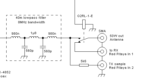 Broadband
RF amplifiers inevitably require lowpass filters to meet spectral
purity requirements. And particularly if they will be driven into some
degree of saturation! I have been in contact with a few hams who are
trying to build linear amplifiers that are naturally clean enough to
meet regulations without such filters, but this is an elusive
goal. At the end of the day, lowpass filters are still the
simplest, cheapest and most efficient way to get the harmonics low
enough.
Broadband
RF amplifiers inevitably require lowpass filters to meet spectral
purity requirements. And particularly if they will be driven into some
degree of saturation! I have been in contact with a few hams who are
trying to build linear amplifiers that are naturally clean enough to
meet regulations without such filters, but this is an elusive
goal. At the end of the day, lowpass filters are still the
simplest, cheapest and most efficient way to get the harmonics low
enough.
I was too lazy to build a whole bank of lowpass filters, one per band
or at least one per octave, with relay switching. Since almost all of
my HF activity is on 40 and 80 meters, I just built a single 40m
lowpass filter, mounted directly on the amplifier board, and I'm using
the amplifier on the air on 40 and 80 meters. For testing on other
bands I unsolder that filter (just the input and output wires) and
either measure without a filter, or with another filter quickly built on the board. It's very important to note in this context
that testing an amplifier with or without lowpass filter is very
different, and the results of one kind of testing should never be mixed
up with those of the other method. What counts is the tests done with
the correct lowpass filter. Any tests done without a lowpass filter are just additions, useful to test
for some specific problems.
I used an inductive-input (T-layout) filter with a low-ripple Chebyshev
response. It has nice standard values for capacitance, by
slightly
tweaking the cutoff frequency, but I still didn't have suitable 560pF
capacitors, so I had to use combinations in parallel. Murphy never
sleeps. The inductors are air-wound, for simplicity, adjustability and cheapness.
Please note that it's definitely not a matter of personal preference
whether to use a T filter or a π filter! The correct type of filter to
use depends on the amplifier type. Transistors are controlled current
sources, so a linear amplifier working without feedback forces the
output current while being voltage-flexible. This is a good match to π
filters, because they tend to force the voltage waveform but accept any
strange current waveform. But when strong negative feedback is added to
a linear amplifier, it behaves very close to an RF voltage source,
forcing the voltage while being current-flexible. Such an amplifier requires T
filters, which force the current waveform and accept the voltage
waveform forced by the amplifier.
If an amplifier is used in hard saturation, it's important to
understand whether it will clip the voltage or the current while
staying in saturation, as this will determine the type of filter to use.
That means, voltage-switching class D amplifiers need T filters, while
current-switching class D amplifiers need π filters.
And when a linear amplifier is slightly driven into saturation, the
type of filter required might change when it saturates! It's important
to avoid this situation. Linear amplifiers that degrade into
voltage-switching class-D when saturating should use strong negative
feedback, to always be voltage sources, while linear
amplifiers
that degrade into current-switching class D when saturating shouldn't
use direct negative feedback. Source degeneration would be OK, though.
Using an amplifier with the wrong type of lowpass filter results in
much lower efficiency! This lurking dragon has bitten many circuit
designers!
For a lowpass filter to have the desired effect on the amplifier, it's
essential that the filter is close enough to the MOSFETs, in terms of
electrical wavelength at the strongest harmonics. This is easy to
achieve with a conventional transformer on the lower bands. It starts
becoming a problem on the higher bands, and is a big problem when using
transmission line transformers or outboard lowpass filters. In those
situations many designers find that they need to use diplexer filters,
adding complexity and loss.
In the configuration I use my 50W amplifier on the air, with the 40m
lowpass filter directly on the board, behind a relatively small
conventional transformer, I have an easy and almost ideal situation,
which facilitates getting high performance.
The lowpass filter is followed by a simple relay for antenna switching.
During RX the antenna is passed over to the Red Pitaya's input #1.
There is also an ultra simple voltage divider, consisting just of a
5.6kΩ resistor and the 50Ω load that's connected to it, to
provide
a sample of a suitable level to the input #2 of the Red Pitaya, which
can be used to provide RF feedback for adaptive predistortion
of
the drive signal. This results in an extremely clean transmitted signal,
and allows some other tricks, as I will explain near the end
of
this page. For now, let's leave the predistortion turned off, and treat
this amplifier as a standard linear one.
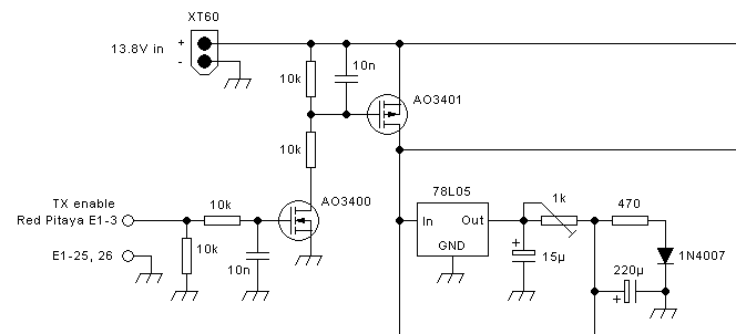 TX/RX
switching is controlled by an auxiliary output of the Red Pitaya, that
works at 3.3V CMOS levels. A very basic two-stage switching circuit,
using tiny but very capable N-channel and P-channel MOSFETs, controls
the power supply to the driver stage, the final stage's bias circuit,
and the relay coil. RC lowpass filtering is included to keep the little
FETs from embarking in any mischief if there is RF pickup. It also
moderates the inrush current charging the bypass capacitors.
TX/RX
switching is controlled by an auxiliary output of the Red Pitaya, that
works at 3.3V CMOS levels. A very basic two-stage switching circuit,
using tiny but very capable N-channel and P-channel MOSFETs, controls
the power supply to the driver stage, the final stage's bias circuit,
and the relay coil. RC lowpass filtering is included to keep the little
FETs from embarking in any mischief if there is RF pickup. It also
moderates the inrush current charging the bypass capacitors.
It seems that the day I designed this switching circuit I wasn't very
creative regarding component values...
As long as the TX enable input is low the entire circuit consumes no
power, doing away with the need for a power switch.
The bias circuit consists of a small 5V regulator, followed
by an
adjustable voltage divider with a slight temperature compensation
provided by a diode. The resistor values are low enough to provide a
low bias source impedance, which is further lowered in the audio and LF
ranges by an electrolytic capacitor, an in the HF and higher
ranges by a ceramic bypass capacitor located at the center tap of the
interstage transformer.
The temperature compensation provided by the single diode is
insufficient to fully compensate drift when the LDMOSFET warms up, but
is good enough for practical operation. When warm, the idling current
might be 10% higher than when cool. It might be better to use two
diodes in series, and reduce the value of the 470Ω resistor, to get
more complete thermal compensation.
I used a very slow, old and common high voltage rectifier diode here,
because it's placed right on top of the LDMOSFET, exposed to a
significant RF field. This diode is simply too slow to rectify
that RF, so there
will be no problem.
I used an XT60 connector for the 13.8V input. I got to know these in
the model aircraft world. They are inexpensive, compact, capable of
carrying 60A, and very good. They are tremendous overkill in this
amplifier, but I think that it's a good standard to use for low
voltage, moderate to high current connections in the ham shack.
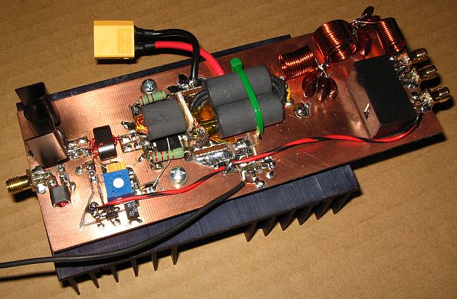
Construction
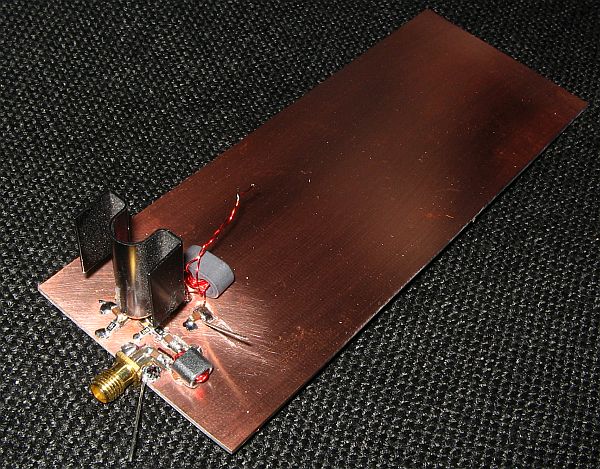 This
amplifier isn't build on a PCB. Instead I built it on a GCB: A gnawed
circuit board! I commissioned a rat to gnaw it for me. That rat has "Dremel"
printed on its back. The background of this decision is twofold: One is
that I temporarily lost my capability for making PCBs, because - again!
- my umpteenth inkjet printer failed and my laser printer absolutely
refuses to make decent PCBs, and the other is that in my old age (55,
but I feel like 85) I have increasing trouble concentrating for long
enough to imagine a whole project in my head and design a board for it
in one pass.
This
amplifier isn't build on a PCB. Instead I built it on a GCB: A gnawed
circuit board! I commissioned a rat to gnaw it for me. That rat has "Dremel"
printed on its back. The background of this decision is twofold: One is
that I temporarily lost my capability for making PCBs, because - again!
- my umpteenth inkjet printer failed and my laser printer absolutely
refuses to make decent PCBs, and the other is that in my old age (55,
but I feel like 85) I have increasing trouble concentrating for long
enough to imagine a whole project in my head and design a board for it
in one pass.
So I got my rat by the tail, grabbed a piece of double-sided PCB/GCB
stock, and had the buzzing animal gnaw my board step by step, stage for
stage, area by area, as construction progressed.
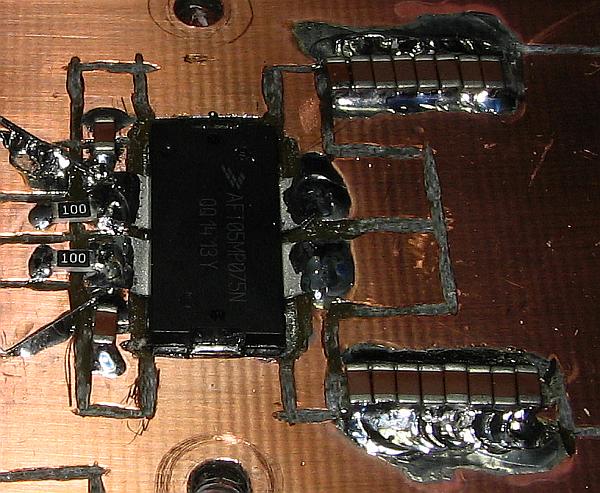
This photo shows the driver stage, temporarily with a
different,
simpler output transformer, fully operational for testing and approving
before continuing the construction.
I decided to use mostly SMD components because they are cheap, good for
RF, and over the years I have collected enough of them to be able to
largely build circuits using them. Some arrived as gifts, others
were bought. I have standardized on the 1206 size as much as possible,
because I can handle and solder them using just a strong magnifier.
Smaller ones would require a microscope...
It would have been nice to use an SMD transistor instead of the old
leaded, metal-cased one,
but there are few, and not as good as the 2N5109. If you absolutely
must use an SMD transistor, you could try the PZT2222A, but its
dissipation rating is very tight for this application, and its
transition frequency is much lower, so it will probably have a very
noticeable gain fall-off on the higher bands. The old 2N5109 is
certainly much better.
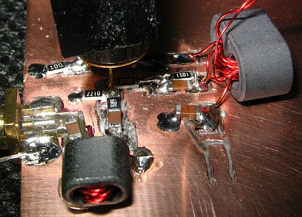 Please
excuse my rat for the unclean gnawing. The rat driver is old and can't
see very well, even when using a magnifier. For the same
reason,
please excuse my soldering iron for doing a sometimes messy job. The
circuit works, and that's good enough at this stage of life.
Please
excuse my rat for the unclean gnawing. The rat driver is old and can't
see very well, even when using a magnifier. For the same
reason,
please excuse my soldering iron for doing a sometimes messy job. The
circuit works, and that's good enough at this stage of life.
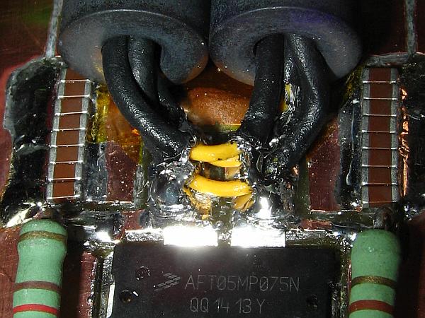
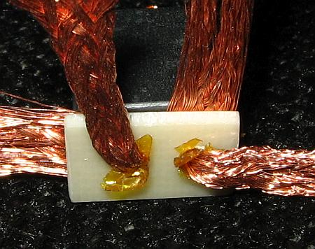
Some details of the output transformer wiring can be seen here quite
clearly. The shorter you get those wires, the better, although a few
extra millimeters aren't a big problem, given the comfortable
impedance
this transformer works at.
Note that I kept the groundplane as continuous as possible, leaving
copper ground bridges in place between parts and under some parts. This
allows getting away without drilling holes to connect to the underside
of the board. If you are less lazy than I am, then be so good and place
a connection through the board at each of those places where something
connects to ground. Specially the bypass capacitors at the
supply
point and at the emitter. It might cause a tiny performance improvement
at the high frequency end.
The transformers can be stuck to the board using hot glue, or double-sided foam tape.
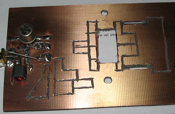 My rat was very happy to
get that much board to gnaw. It's the whole layout for the power stage
and bias circuit.
My rat was very happy to
get that much board to gnaw. It's the whole layout for the power stage
and bias circuit.
The big cutout is for the LDMOSFET, of course, and the round holes are
for screws that will mount the whole assembly to a heatsink. But pay
special attention to the two slits, gnawed out with a Dremel cut-off
wheel. I soldered strips of copper tape through these slits, to get a
very low impedance connection between the top side and the bottom side
ground foils there. The performance of a true class AB amplifier stands
and falls with this. The drain bypass capacitors need to provide a low,
very low, really truly
low inductance connection to the LDMOSFETs source.
If you have a board made by a PCB company, place at least two tightly spaced
rows of vias along these lines, instead of the slits.
 After
soldering the copper tapes into the slits, I soldered 8 bypass
capacitors along each slit, to get a nice low impedance there, and to
distribute the current so that the caps can handle it.
After
soldering the copper tapes into the slits, I soldered 8 bypass
capacitors along each slit, to get a nice low impedance there, and to
distribute the current so that the caps can handle it.
Many builders don't realize how high the RF current in a
class AB
push-pull amplifier's bypass capacitor is! Until it's too late, that
is, until the underrated caps they use blow up. More usually than not,
the maximum current for a cheap SMD capacitor isn't specified. The
options a ham has are to either pay premium prices for RF-rated
capacitors, or do what I did: Use so many in parallel that
trouble
is unlikely. They are cheap enough!
This LDMOSFET is designed to be mounted through boards that are only
0.8mm thick, half of the normal thickness of traditional PCBs.
Since I don't have any such board material, but I do have a large
amount of high quality 1.6mm thick board stock that was given to me by
a fellow ham from the USA, I used some of that, and had my rat gnaw
45-degree chamfers along the edges of the cutout where the
transistor tabs end up. After soldering the transistor to the
heat spreader I bent and soldered down the tabs. It's definitely not
the best way to solve this problem, so if you can get 0.8mm board for
this project, get it.
The heat spreader is a 50mm long piece of 40×5mm silver-clad copper bus
bar, which I also got for free from a friend. Bus bar is a great
material for this purpose, because it's high purity copper and has nice
flat surfaces. Silver plating is nice to have, as it eases the
soldering job, but it's not required. I cut, deburred and drilled that
piece, then drilled the holes in the GCB by using the
spreader as
a template (lazy man's method to avoid measuring).
The spreader doesn't need to be this large and thick. 40×30×3mm would be plenty. I just used what I had.
To solder the transistor and the spreader to the board, I cleaned
everything, applied solder paste to the whole spreader surface, then
screwed the spreader to the board using long spring-loaded screws, then
clamped the board in a horizontal position, placed the transistor in its
hole (correctly oriented!), then heated up the spreader from below,
using a small jeweler's blowtorch. It smoked like an old steam engine,
then the solder melted, the spreader seated itself snugly against the
board's underside, some solder squeezed out, and the transistor of
course followed the laws of molecular attraction, and those of Murphy,
and snugged up as much as it could to one corner. I had to use some tools
to push it into a more suitable location and hold it down there while
the solder solidified. I don't know whether there are solder voids, but
I don't think so, because the flux seems to have almost fully
evaporated, and it seemed to come out of the joint before the solder
did. In any case this transistor has a very generous dissipation
rating, the copper heat spreader I used is also very generously sized
for this power level, so I have no worries about overheating the
transistor in use.
This sort of fully soldered mounting achieves the best possible thermal
and electrical conductivity. It's very much better than alternative
methods in which the spreader isn't soldered to the board.
Also
this is a very solid, robust and simple assembly.
Should it ever become necessary to replace the transistor, this can be
done by removing the board from the heatsink, cutting off the
transistor tabs, heating the spreader, picking off the transistor
corpse, sucking up old solder, then letting the thing cool. Then remove
the tabs, clean everything, apply fresh solder paste to the transistor
mounting area, put the new transistor in place, and reheat the spreader.
Note that I soldered wire jumpers from the gate areas to ground, to
protect the LDMOSFET gates during all this work. Better safe than
sorry.
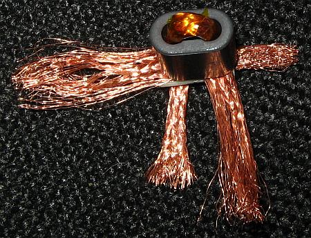
 The
next step was building and installing the output transformer. It has 3
turns of 25Ω coax cable, starting and ending on the output
side. On the input side the braids of all three turns are cut,
and
soldered to the LDMOSFET drains as shown here, to form a single-turn
primary winding consisting of the three parallel-connected braids.
The
next step was building and installing the output transformer. It has 3
turns of 25Ω coax cable, starting and ending on the output
side. On the input side the braids of all three turns are cut,
and
soldered to the LDMOSFET drains as shown here, to form a single-turn
primary winding consisting of the three parallel-connected braids.
My intentions were nicer than the outcome. I intended to place the
three turns nicely and orderly against the board, like three U shapes
nestled into one another. But the rather stiff coax cable, my even stiffer
arthritic fingers, and my old and presbioptic eyes decided otherwise.
It looks messy, and it is, but it ended up correctly connected...
This method of connecting the primary side minimizes leakage
inductance.
On the output side two of the turns simply loop, while the third one is
the start and end of the secondary winding. The center conductor of the
ends is connected to ground and the output point, while the two braid
ends are soldered together.
The outer insulation of the coax cable isn't
electrically required. The transformer would work the same if
the
three braids were in random contact along their whole length, or even
soldered together. I used an outer layer only to hold the braid tightly
to the dielectric, to keep the cable's impedance from rising.
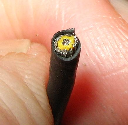 25Ω
coax cable can be bought ready-made, but only from specialist
companies, and at prices that are much stiffer than the cable. For that
reason I made my own. I used a piece of stranded, silver-plated,
teflon-insulated wire, having an overall diameter of 1.3mm, and pulled
the braid of some good quality RG-174 cable over it. Then I pulled a
very tightly fitting heat shrink tube over that, and heated it. The
result is a coax cable that should have roughly the correct impedance,
thanks to the wire being much thicker than RG-174's center conductor,
the other dimensions being about the same. I didn't measure the actual
impedance of this cable, but anyway it's not terribly critical, given
that the total length of the three turns is only about 28cm.
25Ω
coax cable can be bought ready-made, but only from specialist
companies, and at prices that are much stiffer than the cable. For that
reason I made my own. I used a piece of stranded, silver-plated,
teflon-insulated wire, having an overall diameter of 1.3mm, and pulled
the braid of some good quality RG-174 cable over it. Then I pulled a
very tightly fitting heat shrink tube over that, and heated it. The
result is a coax cable that should have roughly the correct impedance,
thanks to the wire being much thicker than RG-174's center conductor,
the other dimensions being about the same. I didn't measure the actual
impedance of this cable, but anyway it's not terribly critical, given
that the total length of the three turns is only about 28cm.
I used two Amidon FB-61-4852 ferrite sleeves, which give plenty enough
inductance for 160m, more than enough voltage handling for 13.8V
operation at low loss, and also can handle considerable DC without
saturating. Given that no DC blocking capacitor is used, any small
difference in the resistances of both sides of the feed transformer
will result in a DC flowing in the output transformer's primary, so this point
needs to be considered. Don't replace these cores by any having a higher
permeability!
The three turns of coax cable fit tightly through the holes of
these cores.
 The
feed transformer of a class AB push-pull amplifier has the duty to
tightly couple the drains, and at the same time bring in the power
supply in a way that allows the huge second harmonic supply current
ripple to go through to the bypass capacitors. It needs to have
extremely low leakage inductance, and the circuit it works in, which
includes the transistors, the bypass caps, and all their
interconnections, including the path through ground, must also
have extremely low stray inductance. A class AB linear amplifier of
this kind works well in the frequency range where these leakage and
stray inductances are negligible. At higher frequencies these
inductances cause trouble, making the amplifier's performance degrade.
The
feed transformer of a class AB push-pull amplifier has the duty to
tightly couple the drains, and at the same time bring in the power
supply in a way that allows the huge second harmonic supply current
ripple to go through to the bypass capacitors. It needs to have
extremely low leakage inductance, and the circuit it works in, which
includes the transistors, the bypass caps, and all their
interconnections, including the path through ground, must also
have extremely low stray inductance. A class AB linear amplifier of
this kind works well in the frequency range where these leakage and
stray inductances are negligible. At higher frequencies these
inductances cause trouble, making the amplifier's performance degrade.
Many people have used bifiliar
chokes using several turns of two parallel wires wound on toroidal
cores. Those do not work!!! Or rather, they do bring in the DC just
fine, of course, and being bifiliarly wound they benefit from DC
cancellation, which keeps them from saturating - but that's all. They
don't couple the drains, because their leakage inductance is far too
high. In that regard they work almost exactly like two separate feed
chokes. My amplifier instead attempts to demonstrate the advantages of
getting this point as correct as possible.
To this end I picked the smallest ferrite core that can just barely
handle the voltage at low enough loss on the lowest band (160m), and
that provides just barely enough inductance on that band. A good choice
of core material, size and shape is required. Unfortunately the choice
of ferrite materials a private experimenter can obtain is extremely
limited. Among the cores I can get, the Amidon BN-61-202 was the most
promising.
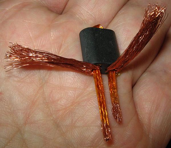
I wound this core with a single turn of homemade extra low impedance
coax cable. The point here is getting the insulation so thin that the
two conductors end up very close together, minimizing leakage
inductance. I used braid from a good quality RG-58 cable, wrapped one
piece of that braid in a spiral winding of kapton tape, wound with such
an overlay as to get two layers of tape covering the conductor.
Then
I slipped another piece of identical braid over it, and wrapped it in
kapton tape just to keep that braid in close contact with the
insulation.
 The
outer braid ends were bent to the sides, and the inner ones were
threaded through the holes drilled into a piece of copper-free PCB
material, used as insulating separator. The kapton wrap goes along into
the holes, to maintain integrity of insulation, and then was cut.
The
outer braid ends were bent to the sides, and the inner ones were
threaded through the holes drilled into a piece of copper-free PCB
material, used as insulating separator. The kapton wrap goes along into
the holes, to maintain integrity of insulation, and then was cut.
 This
is the somewhat uncombed feed transformer, ready for installation. My
idea was that after soldering the three coax loops of the output
transformer flat to the drain pad, I would solder the very short feed
transformer terminals to the top side of those coax cables, and bend
the feed transformer side terminals down to the bypass capacitors,
fanning them out to minimize inductance, and solder them. The core
would stand vertically over the drain pad area.
This
is the somewhat uncombed feed transformer, ready for installation. My
idea was that after soldering the three coax loops of the output
transformer flat to the drain pad, I would solder the very short feed
transformer terminals to the top side of those coax cables, and bend
the feed transformer side terminals down to the bypass capacitors,
fanning them out to minimize inductance, and solder them. The core
would stand vertically over the drain pad area.
 As
happens so often, practice ended up differing somewhat from theory. My
rat had left rather little space there, and my old eyes and hands had
made a mess with the transformer connections, so that I had to change
plans and install the feed transformer in the best way I found at that
point. It ended up roughly horizontal over the LDMOSFET, with much
longer supply terminals than I intended. There are several
nanohenries of stray inductance here, which weren't planned. Just the
feed transformer's terminal inductance is surely much larger
than its leakage inductance. Those two act in series and are
equally undesirable.
As
happens so often, practice ended up differing somewhat from theory. My
rat had left rather little space there, and my old eyes and hands had
made a mess with the transformer connections, so that I had to change
plans and install the feed transformer in the best way I found at that
point. It ended up roughly horizontal over the LDMOSFET, with much
longer supply terminals than I intended. There are several
nanohenries of stray inductance here, which weren't planned. Just the
feed transformer's terminal inductance is surely much larger
than its leakage inductance. Those two act in series and are
equally undesirable.
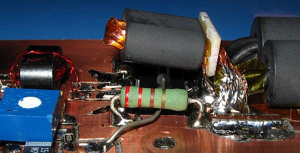
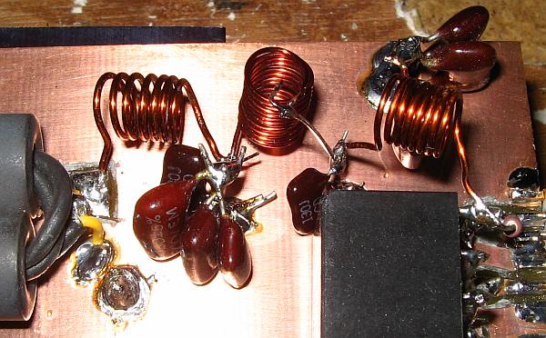
Note that in this photo you can see the temperature sensing diode lying
on the LDMOSFET, and the drive transformer is in place. The gate
shorting jumpers have been removed.
The 3W feedback resistors are far larger than necessary. 1W would have
been just big enough, but I had none. I found these big 220Ω resistors
on old CRT TV boards. Two separate TVs, so the two resistors aren't
identical, but they are of the same value, type and size!
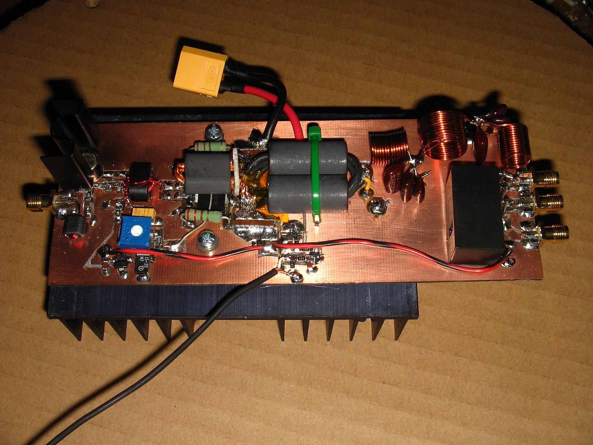
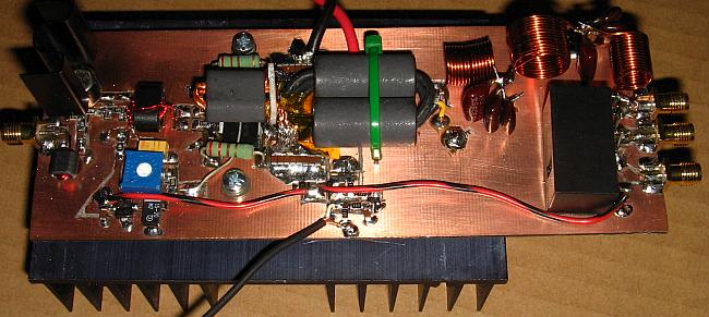 After
some more board gnawing, building the TX/RX switching circuit, the low
pass filter, installing the relay and
the
output-side connectors, and bolting the whole thing to a heatsink, it
looked like this. You can click this photo to get a larger version and
see the amplifier in its full glory.
After
some more board gnawing, building the TX/RX switching circuit, the low
pass filter, installing the relay and
the
output-side connectors, and bolting the whole thing to a heatsink, it
looked like this. You can click this photo to get a larger version and
see the amplifier in its full glory.
The relay I used is far larger than necessary for this low power. It comes from the parts
I bought for the legal-limit power project.
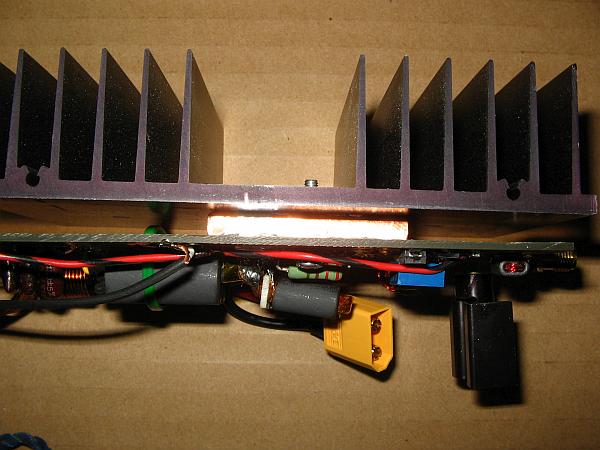 Here
is a view that shows the spreader between the heatsink and the
board. The heatsink measures 120×75×30mm, and during ragchewing at full
power it gets just lukewarm. Without needing a fan, of course. During long
term key-down testing it gets somewhat warmer, but not a lot.
Here
is a view that shows the spreader between the heatsink and the
board. The heatsink measures 120×75×30mm, and during ragchewing at full
power it gets just lukewarm. Without needing a fan, of course. During long
term key-down testing it gets somewhat warmer, but not a lot.
The copper foil connecting the bypass caps to the underside foil ends
up sandwiched between the board and the heat spreader. For that reason
the board doesn't sit exactly parallel to the heatsink. Its output side sits
higher than the input side. The solder fills out the resulting space
between the board and the spreader.
Given the stiffness of this board, no additional support was fond
necessary. It's attached to the heatsink just by the two screws.
There are no connections on the underside of the board. It's just a
continuous groundplane joined to the upper side groundplane only at the
connectors and through the two copper tape straps. Some more
interconnections might improve performance on the high bands.
Performance measurements
I used digital multimeters to measure the supply voltage and current. A
Tektronix 485 oscilloscope with either direct 50Ω connection through
attenuators, or using low impedance Z0 probes having over 500MHz bandwidth, to see the waveforms and
to measure the output power. And the spectral display of PowerSDR,
derived through receiver #2 from the feedback voltage divider, to
assess linearity through IMD measurement. The software's adaptive
predistortion amplifier analyzer was used to separately measure and
graph amplitude and phase linearity. The 50Ω dummy load used is a Bird
unit rated up to UHF.
All measurement results are for the complete amplifier, including the
driver stage. The driver, relay, switching circuit and bias circuit
draw a total of 120mA, so that the current in the final stage is always 0.12A lower
than the total current.
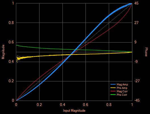
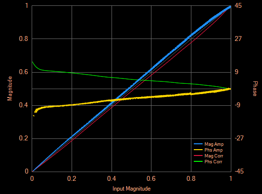
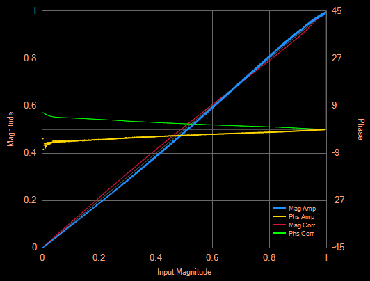 On the 40m band, using
the 40m lowpass filter, a 13.8V
supply, and with the bias set for 1.12A total current at no drive (1A
in the final stage), the amplifier just begins compressing the gain at
50W output. These curves show the amplifier's response under these
conditions. The blue curve is the amplitude response, and the yellow
curve shows the phase response. The other two curves are the
compliments to them, and show the corrections that the adaptive
predistortion system will apply if switched on.
On the 40m band, using
the 40m lowpass filter, a 13.8V
supply, and with the bias set for 1.12A total current at no drive (1A
in the final stage), the amplifier just begins compressing the gain at
50W output. These curves show the amplifier's response under these
conditions. The blue curve is the amplitude response, and the yellow
curve shows the phase response. The other two curves are the
compliments to them, and show the corrections that the adaptive
predistortion system will apply if switched on.
As you can see, the gain curve is quite linear, but not perfectly so,
showing lowest gain at about one third of the maximum amplitude, and
highest gain at a little less than full power. This sort of distortion
is inevitable, given that MOSFETs are square-law devices, rather than
linear ones. We could eliminate the slight nonlinearity at the high end
of the drive range, by limiting the amplifier to 45W, or by slightly
increasing the supply voltage, but the distortion in the low power
range is simply a fact of life. We can reduce it, by further increasing
the bias and by using even stronger negative feedback, but never
eliminate it.
The phase response shows roughly 6° phase shift between low power
and maximum. This comes mostly from the voltage-variable capacitances
all transistors have, and we cannot do much about it except choosing
transistors that have low capacitances, which I did.
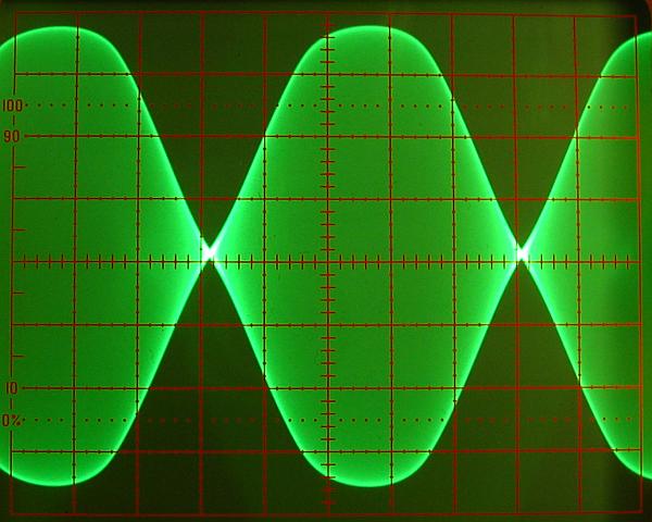
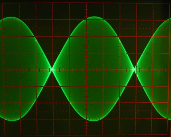
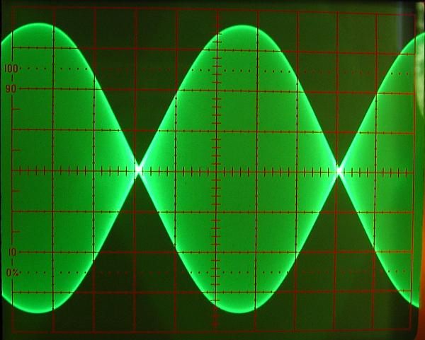 The
two-tone signal looks pretty clean and nice on the scope screen. It
would take a very well trained eye to detect the slight amplitude
distortion of this amplifier on the scope! And of course the
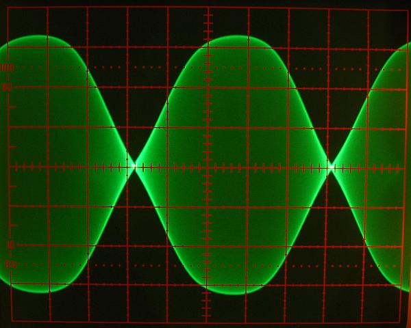
scope can't show the phase distortion at all.
The
two-tone signal looks pretty clean and nice on the scope screen. It
would take a very well trained eye to detect the slight amplitude
distortion of this amplifier on the scope! And of course the
scope can't show the phase distortion at all.
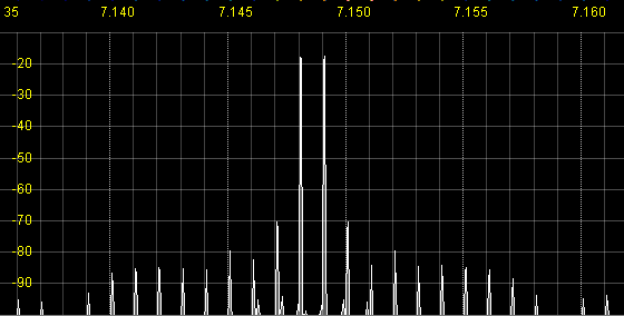
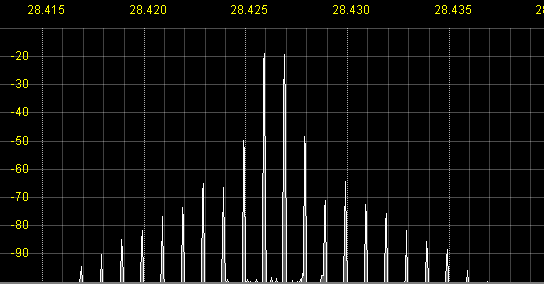
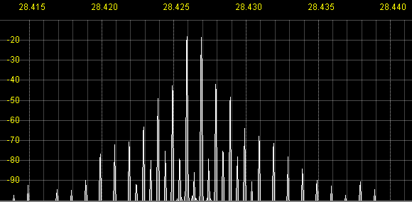
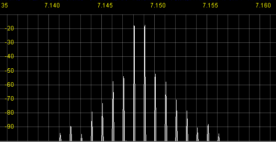 The
spectrum analyzer is the best tool to assess linearity. You can see
that the third order intermodulation products are roughly 34 or 35dB
below the individual tones, which means that they are 40 to 41dB below
the PEP output. This is much better than what many commercial
transceivers achieve!
The
spectrum analyzer is the best tool to assess linearity. You can see
that the third order intermodulation products are roughly 34 or 35dB
below the individual tones, which means that they are 40 to 41dB below
the PEP output. This is much better than what many commercial
transceivers achieve!
The 5th order IMD is only slightly lower, but the higher IMD products
fall off in strength rather quickly.
Operating under these conditions, the complete amplifier draws 3.74A.
At 50W single tone (carrier) output, it draws 5.57A. That's a
single-tone efficiency of 65% for the entire amplifier, including the
driver and switching, or 66.5% for the final stage alone.
The theoretical limit for pure class B amplifiers is 78.5%, but in real
amplifiers it's always lower due to imperfect saturation of
the
transistors, and various other losses. Class AB further reduces the
efficiency. So the efficiency this little amplifier is producing is
probably as good as one could hope for!
 Although
this amplifier is plenty clean enough to put it on the air without any
digital tricks, there is no reason why I shouldn't use some of the
trickery offered by modern digital signal processing. Among these is
adaptive predistortion. Switching it on makes the 3rd IMD plummet to
53dB below each tone, 59dB below PEP, and all other IMD products are at
least a further 10dB down! The PEP output increases in a barely
noticeable way, and the total supply current increases
marginally
to 3.79A.
Although
this amplifier is plenty clean enough to put it on the air without any
digital tricks, there is no reason why I shouldn't use some of the
trickery offered by modern digital signal processing. Among these is
adaptive predistortion. Switching it on makes the 3rd IMD plummet to
53dB below each tone, 59dB below PEP, and all other IMD products are at
least a further 10dB down! The PEP output increases in a barely
noticeable way, and the total supply current increases
marginally
to 3.79A.
Not all IMD products shrink, though. The more remote ones, starting at
with the 11th, actually increase in strength, compared to the
non-predistorted result. This is a typical side-effect of predistortion
in digital processing, caused mainly by the limited bandwidth
over
which the predistortion system analyzes and corrects the amplifier's nonlinearities. But with all
these rogue IMD products being much more than 60dB below PEP, it's a
non-issue in most practical ham applications.
 Having
the adaptive predistortion system at my disposal, it's of course
tempting to improve the amplifier's efficiency and output
power, worsening its linearity in the process, and then fix up
the
linearity through that digital magic. To try this, I reduced the bias
setting to get only 0.5A total current draw at no signal, meaning 380mA
idling current in the final stage, and then driving it more strongly, all
the way into pretty deep gain compression.
Having
the adaptive predistortion system at my disposal, it's of course
tempting to improve the amplifier's efficiency and output
power, worsening its linearity in the process, and then fix up
the
linearity through that digital magic. To try this, I reduced the bias
setting to get only 0.5A total current draw at no signal, meaning 380mA
idling current in the final stage, and then driving it more strongly, all
the way into pretty deep gain compression.
This being a clean class AB push-pull amplifier, which clips the output
voltage when overdriven, the gain compression is rather hard and abrupt, so there
is only a modest amount of power to be gained by operation in saturation. I got 61W output while
operating the amplifier in this way.
The gain curve shows strong compression at high power, and rather
severe crossover distortion caused by the low bias. The phase response curve instead doesn't
change much, there is just a little more phase change in the saturation
region, caused by the drains getting closer to ground potential for a
larger portion of the RF cycle. At lowest drain voltage the capacitance
modulation is greatest.
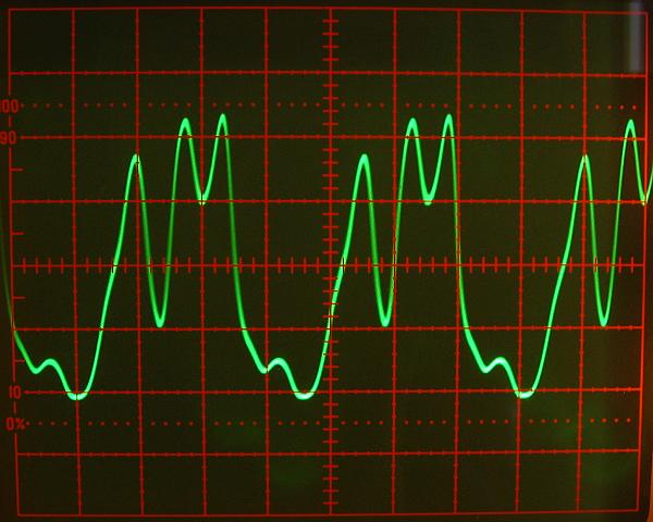
 The
waveform on the scope screen shows both the crossover distortion and the
flat-topping in a very obvious way. It's easy to see the distorted
amplitude response curve modulating the sine envelope!
The
waveform on the scope screen shows both the crossover distortion and the
flat-topping in a very obvious way. It's easy to see the distorted
amplitude response curve modulating the sine envelope!
How dirty is such a signal?
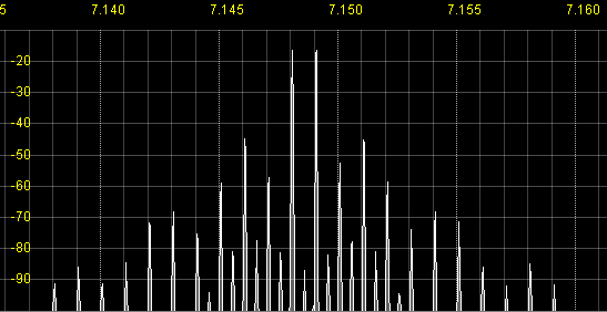 The spectrum
analyzer provides the answer: Much more dirty! But plenty good enough
for some people...
The spectrum
analyzer provides the answer: Much more dirty! But plenty good enough
for some people...
The 5th IMD ends up larger than the 3rd one, at about 28dB below each
tone. Sneaky specmen wanting to sell an amplifer that normally works
like this might proudly tell you that the 3rd IMD is 35dB down,
without telling you that the 5th IMD is only 28dB down!
Most manufacturers are fully satisfied with such a result, and
many commercially available transceivers cannot do better
than this when driven to their full output! Specially at lower than normal supply voltage.
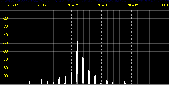
 Using
PowerSDR, I can. You can too, if you use it. Switching on the adaptive
predistortion pushes the IMD products down where they belong! The
3rd IMD is down about 52dB below each tone, barely 1dB worse
than
at 50W with high bias!
Using
PowerSDR, I can. You can too, if you use it. Switching on the adaptive
predistortion pushes the IMD products down where they belong! The
3rd IMD is down about 52dB below each tone, barely 1dB worse
than
at 50W with high bias!
Operating like this, with predistortion, the amplifier produces a very
clean 61W signal, while consuming 4.03A during 2-tone transmission,
and 5.97A when transmitting a single tone (carrier). And
that,
dear folks, is 74% overall efficiency, including the driver stage,
relay and switching circuit! Or 75.6% if we only measure the final
stage's current drain, but I won't put my hand on fire for the
decimals, given that I'm measuring the power on a scope screen.
Although my scope is of high quality, very well calibrated, and
produces a nice sharp trace, analog measurement has its
limits...
Getting ~75% efficiency from a very simple class AB amplifier, along
with a very clean signal, is strong advertising for adaptive
predistortion and for clean amplifier design.
I tried to go further, by turning down the bias even lower, driving the
amplifier even harder, and letting the adaptive predistortion clean up
the resulting mess. But the results were not so nice, because the low
bias made the far-out IMD products rise, and these are out of the
control of the bandwidth-limited adaptive predistortion system. It can
do magic only up to a point... So I concluded that
operating the amplifier like shown here, at slightly over 60W and with
0.5A total current at zero signal, and using adaptive predistortion, is
about best. And for people who don't have a signal generating system
that includes adaptive predistortion, I suggest to keep the bias
setting at about 1.1 to 1.3A total current at no signal, and limit the
output power to 50W.
Nothing had been said so far about harmonics, because thanks to the use
of a decent lowpass filter they aren't an issue. But I quickly measured
them. Running the amplifier at 61W output, the second harmonic is 54dB
down from the fundamental, the third one is 63dB down, the fourth is
77dB down, and the fifth is 74dB down. Push-pull amplifiers suppress
self-generated even harmonics, if they are well balanced, but
of
course they happily amplify any harmonic that might be present in the
driving signal! And my driver stage is single-ended, so the second
harmonic is its strongest. Also the Red Pitaya might have some significant harmonic
contents in its output. These are the reasons why the second harmonic
is the strongest by far. Combined with the fact, of course, that
lowpass filters attenuate higher harmonics more strongly.
If some stringent application would require stronger suppression of the
second harmonic, I would try a push-pull driver stage.
 In
broadband RF amplifiers the voltage waveform at the drain usually
reveals such severe imperfections that many builders prefer not looking
at it! Since I seem to have masochist inclinations, at least in the
realm of electronics, I do.
In
broadband RF amplifiers the voltage waveform at the drain usually
reveals such severe imperfections that many builders prefer not looking
at it! Since I seem to have masochist inclinations, at least in the
realm of electronics, I do.
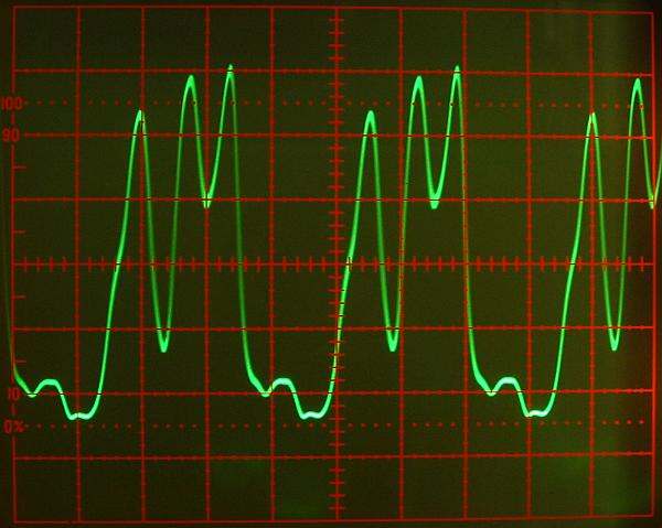
At roughly 20W output power, it looks as shown here. The vertical scale
is 5V/div, and the screen center is at the 13.8V supply voltage. As you
can see, the waveform closely resembles a sine wave, except for
a wiggle at zero-crossing time, when the transistor is ceasing
conduction. This is caused by the non-zero leakage and stray
inductance in the feed transformer and associated circuit. As much as I
tried to reduce these unwanted inductances, a few tens of nanohenry
remain, and at the low drain load of just around 1.4Ω on the active
side, that's bad enough.
Even with this wiggle, this waveform is much better than what you will
see in many other push-pull amplifiers.
 At 61W
output the amplifier is strongly saturated. You can see the LDMOSFET
pulling its drain very close to ground, roughly 0.5V (remember that the
center line is 13.8V and scale is 5V/div).
At 61W
output the amplifier is strongly saturated. You can see the LDMOSFET
pulling its drain very close to ground, roughly 0.5V (remember that the
center line is 13.8V and scale is 5V/div).
The wiggle is still present and larger, due to the higher drain
current.
It can also be seen that coupling between the drains is present
but
far from perfect. If it was perfect, the waveform would be symmetrical.
But the top of the waveform shows a ramp instead of a horizontal line
while the opposite transistor holds its drain to ground, which
again is caused
by the stray and leakage inductances. At least the coupling is good
enough to totally avoid voltage overshoot. The peak drain voltage is
a little less than twice the supply voltage, exactly like it should be
in a class AB amplifier.
And since leakage inductance is uncoupled between the sides, the wiggle
of one side doesn't transfer to the other. Instead there is a separate,
smaller wiggle on the downgoing slope, caused by the rising drain
current and the leakage inductance.
In the spectral domain these wiggles appear as harmonics, and are
rejected pretty well by the lowpass filter.
So my lovingly crafted feed transformer and my carefully
designed
very low inductance ground return are still bad enough to cause
obviously imperfect drain-to-drain coupling even on 40 meters! While the
7MHz fundamental is well coupled, the harmonics aren't. On higher bands
this can only get worse.
I did much testing on 40m for three reasons: Because the 40m band is
the geometric center of this amplifier's intended bandwidth, being a
factor 4 above the 160m band and the same factor 4 below the
10m
band; Also because it's the band I use most; But mainly
because I
had the 40m lowpass filter installed on the board when I started
doing systematic tests!
 Of course it's essential to see how the amplifier behaves on the other
bands. To avoid having to build a lot of lowpass filters, and
to
abstain from doing measurements without a lowpass filter in place,
which are essentially meaningless because harmonic power masquerades as
useful power and the amplifier operates under totally abnormal
conditions, I built a lowpass filter for 10m,
just for testing.
Of course it's essential to see how the amplifier behaves on the other
bands. To avoid having to build a lot of lowpass filters, and
to
abstain from doing measurements without a lowpass filter in place,
which are essentially meaningless because harmonic power masquerades as
useful power and the amplifier operates under totally abnormal
conditions, I built a lowpass filter for 10m,
just for testing.
The leakage inductance of the output transformer, plus the stray inductance of
the connections between the transformer and the LDMOSFET, are low
enough to be negligible on the 40m band. But not so on 10m! I measured
the leakage+stray inductance by connecting my NanoVNA to the secondary
side of the transformer, while placing a short between the drains,
directly at the FET's body. It came out as 68nH. That's pretty good,
and with proper compensation would allow using this transformer up to
about 100MHz. Compensation is really easy when using a T-configured
lowpass filter, because all that has to be done is subtracting the
leakage+stray inductance from the exact inductance calculated for the
input coil of the filter! With my choices of cutoff frequency and
bandpass ripple I ended up needing 236nH for the filter's
input
inductor without compensation, so I made that inductor to have 168nH,
to compensate for the leakage+stray of the amplifier's output section.
I wound the coils to give a little more than the exact needed
inductance when close-wound, and then stretched them out a little while
measuring their inductances, to get the exact values.
I left the capacitor groups of the 40m filter in place, just removing
its coils, and built the 10m filter around them. Laziness rules.
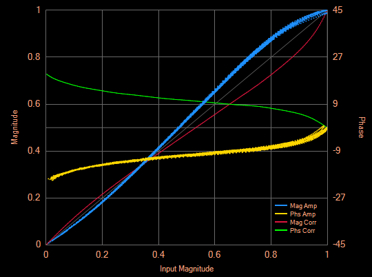
 These
are the amplifier's gain and phase curves on 10m, operating in linear
mode, with 1A idling current in the final stage, and driven to the
point where gain compression starts. At this point it delivers 40W
output.
These
are the amplifier's gain and phase curves on 10m, operating in linear
mode, with 1A idling current in the final stage, and driven to the
point where gain compression starts. At this point it delivers 40W
output.
The amplitude linearity curve is different but not much worse than on 40m. The
phase response instead is significantly worse than on 40m. This is an
inevitable result of the voltage-variable capacitances in
semiconductors having more effect at higher frequencies.
 The
two-tone waveform looks pretty good, since it cannot show phase
distortion. Judging SSB signal quality purely from such a scope display
is misleading, for this reason.
The
two-tone waveform looks pretty good, since it cannot show phase
distortion. Judging SSB signal quality purely from such a scope display
is misleading, for this reason.
Vertical scale is the same as in the 40m tests. The power difference
between the bands is clearly visible. Slightly lower voltage, meaning significantly lower power.
 Without
using any sort of correction, the 3rd IMD products are 30dB down from
the individual tones, 36dB down from PEP. That's about 4 to 5dB worse
than on 40m, but still pretty good. The higher order IMD products fall
off at a slower rate than on 40m, probably mostly an effect of the
phase distortion.
Without
using any sort of correction, the 3rd IMD products are 30dB down from
the individual tones, 36dB down from PEP. That's about 4 to 5dB worse
than on 40m, but still pretty good. The higher order IMD products fall
off at a slower rate than on 40m, probably mostly an effect of the
phase distortion.
Under these conditions the amplifier consumes 4.38A with a two-signal,
and 6.65A with a single tone. That equates to 43.6% efficiency
including the driver stage, a much worse result than the 65% achieved
on 40m in linear operation.
 Enabling
the adaptive predistorstion system cleans up the amplifier to a high
quality, pushing the 3rd IMD down about 46dB below each tone. Again,
not as good as the 53dB obtained on 40m.
Enabling
the adaptive predistorstion system cleans up the amplifier to a high
quality, pushing the 3rd IMD down about 46dB below each tone. Again,
not as good as the 53dB obtained on 40m.
 Reducing
the bias to obtain 0.5A total current drain at zero signal, 380mA in
the final stage, and increasing the drive into stronger saturation,
these are the response curves obtained. The amplitude distortion is
quite similar to the 40m case, only the curve is noticeably noisier. I
don't know how much of this comes from memory effects in the amplifier,
and how much is actual noise, derived from the fewer samples per RF
cycle that the Red Pitaya has to work with, on the higher frequency.
Reducing
the bias to obtain 0.5A total current drain at zero signal, 380mA in
the final stage, and increasing the drive into stronger saturation,
these are the response curves obtained. The amplitude distortion is
quite similar to the 40m case, only the curve is noticeably noisier. I
don't know how much of this comes from memory effects in the amplifier,
and how much is actual noise, derived from the fewer samples per RF
cycle that the Red Pitaya has to work with, on the higher frequency.
The phase distortion also increases, and its trace also looks noisier.
 No
news here, the scope pattern shows the deformation that are
caused
by the amplitude nonlinearity reported in the blue curve above.
No
news here, the scope pattern shows the deformation that are
caused
by the amplitude nonlinearity reported in the blue curve above.
 The
uncorrected signal produced in this way is of course quite dirty: The
3rd IMD is only 23 or 24dB below each tone! This is too dirty to put on
the air without being ashamed.
The
uncorrected signal produced in this way is of course quite dirty: The
3rd IMD is only 23 or 24dB below each tone! This is too dirty to put on
the air without being ashamed.
 Digital
magic to the rescue! With predistortion enabled, the 3rd IMD is again
46dB or so below each tone, an excellent signal quality.
Digital
magic to the rescue! With predistortion enabled, the 3rd IMD is again
46dB or so below each tone, an excellent signal quality.
Under these conditions the amplifier delivers 44W PEP, consuming 4.26A.
Transmitting a single tone it consumes 6.69A, giving 47.7%
efficiency including the driver stage. Poor, but usual for solid state
amplifiers operating at the high end of their frequency range.
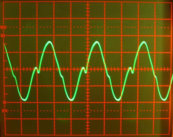
 The
RF voltage waveform at one drain shows why we are getting less power,
more amplitude distortion and much lower efficiency on 10m.
The
RF voltage waveform at one drain shows why we are getting less power,
more amplitude distortion and much lower efficiency on 10m.
This trace was shot with the low bias setting and at a drive level
where the FETs don't saturate. The center line is at the
13.8V supply voltage, scale is 5V/div. The zero-crossing
wiggle
caused by leakage inductance in the feed transformer and connections
has grown to an enormous size, due to the much faster current slew rate
at the higher frequency.
Also an inversion of the positive peak appears, which is another
telltale sign of leakage inductance in the feed transformer. The
amplifier is being current-starved at the signal peaks, due to leakage
inductance acting as a choke in series with the supply, after the
bypass caps.
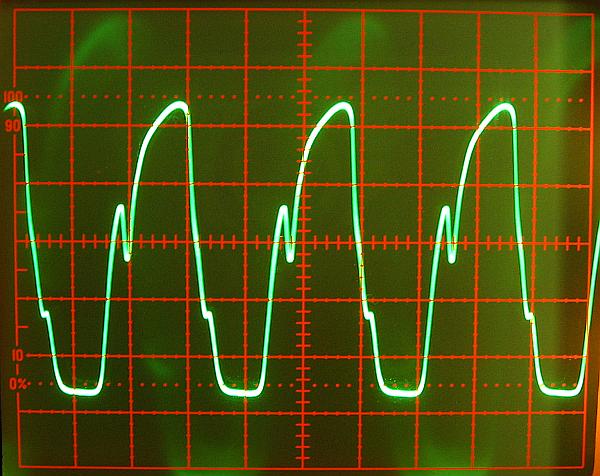
 In
saturated operation we can see that the drain voltage gets pulled down
to about -12V from the supply, meaning about 1.8V drain saturation
voltage. The drain-source capacitance, which gets large at low drain
voltage, has a stronger limiting effect than on 40m. So does the
reverse transfer capacitance of the FETs. This reduced amplitude,
combined with the
very distorted waveform, which contains less fundamental energy, is the
cause why the amplifier delivers so much less power on 10m than on 40m,
even in
saturation.
In
saturated operation we can see that the drain voltage gets pulled down
to about -12V from the supply, meaning about 1.8V drain saturation
voltage. The drain-source capacitance, which gets large at low drain
voltage, has a stronger limiting effect than on 40m. So does the
reverse transfer capacitance of the FETs. This reduced amplitude,
combined with the
very distorted waveform, which contains less fundamental energy, is the
cause why the amplifier delivers so much less power on 10m than on 40m,
even in
saturation.
How could this be improved?
If we could buy better magnetic cores, that have higher permeability
along with low loss at high flux density, we could use them to make an almost
microscopically small feed transformer, that has very low leakage
inductance. This could be embedded right over or under the LDMOSFET
drain tabs, with minimal-length and maximal-width bypass capacitors
and connections to the MOSFET source. But since such a good magnetic material
doesn't exist yet, as far as I know, this remains a purely theoretical
solution.
Many manufacturers and experimenters have done away completely with
the feed transformer, living with totally uncoupled drains, thus
running their amplifiers in a class AB-D hybrid mode. This can work
well if square wave drive is used, but that requires additional care in
the driver stage. All practical implementations of this sort that I
have tested, have ended up showing equal or worse performance than my
little amplifier - and on all bands, not just at the high end of their
frequency ranges! My amplifier at least is good on the lower bands...
Using a higher supply voltage improves the situation. For example at 4 times higher
voltage, and the same power, 4 times as much ferrite cross-section is
needed, thus the feed transformer will have twice the wire length and twice the leakage
inductance, if built in the same style. But the drain load resistance
will be 16 times as high, making us end up with a situation that is 8
times better! In addition the stray inductance in the connections will
probably remain the same, and so the final result will be more than 8
times better. It smells like a good solution. The problem is that RF
power transistors for higher voltages suffer much more from
internal capacitances. Phase distortion can be really bad with them, and the
very existence of those high capacitances, relative to load impedance,
also causes some trouble in getting good efficiency.
Other bands:
I was too lazy to build more lowpass filters, so I tested 20 to 12
meters using the 10m filter, and 160 and 80 using the 40m
filter. For that reason I prefer not publishing detailed per-band test
results, as they would be slightly differenet from what would be
obtained with the correct filters for each band.
But there were no surprises during this testing. The efficiency is a
tad better on 80m than on 40m, while on 160m it gets down again to the
40m value, as the feed transformer starts showing that its inductance
isn't sky-high. Linearity also shows a general trend to be best on the
lowest
bands, caused by the phase distortion being larger at higher
frequencies. Using adaptive predistortion, the signal quality is
excellent on all bands. The bands between 40 and 10m show the
intermediate results that are to be expected, without any odd behavior
on any band. The drain voltage waveform deformations get larger as the
frequency rises. Instead it looks very clean on 160m, where the
leakage and
stray inductances in the feed circuit are small enough to cause almost
no effect.
Harmonic suppression is good enough to meet legal requirements only
when using a suitable lowpass filter. That's true even on 160m. It's
fine to operate on 12m using the 10m filter, even operating on 15m with
the 10m filter still meets requirements, barely, while operating on 17m
with the 10m filter doesn't meet them, with the second harmonic being
suppressed less than 40dB. So an all-band setup using
this amplifier would require switchable filters for 160, 80, 40, 20, 15
and 10m. If a push-pull driver would be used, probably the even-order
harmonics would be low enough to allow eliminating the 15m filter
and meet legal requirements on 17m using the 10m filter.
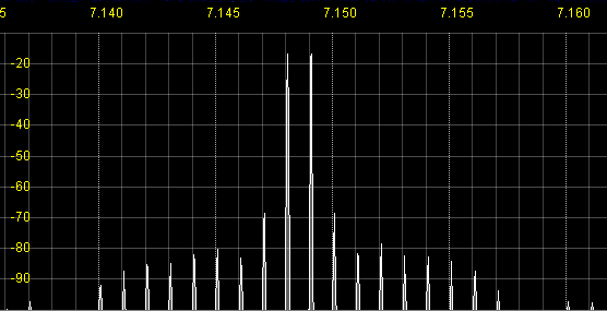
Reality check: The TS-450S
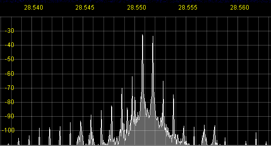 When
testing RF power amplifiers one can easily get depressed. In such cases
it's good to compare to what the competition achieves. Here is a
spectrogram of my Kenwood TS-450SAT's output on 10m. The 3rd
IMD
is down 29 to 30dB from each tone, which is almost as good as the Red
Pitaya with my homebrew amplifier when not using predistortion. But the
Kenwood is worse then my setup regarding the higher IMD products, and
is very much worse in phase noise! Of course, we are comparing
different technological generations here. The TS-450 only
has linear signal processing, with a balanced modulator, an
SSB
filter, several further stages of mixing, and a complex frequency
synthesizer that includes two DDS blocks and several PLLs. The Red
Pitaya setup instead does almost everything digitally,
even the
generation of the dual-tone test signal. That does allow better signal quality.
When
testing RF power amplifiers one can easily get depressed. In such cases
it's good to compare to what the competition achieves. Here is a
spectrogram of my Kenwood TS-450SAT's output on 10m. The 3rd
IMD
is down 29 to 30dB from each tone, which is almost as good as the Red
Pitaya with my homebrew amplifier when not using predistortion. But the
Kenwood is worse then my setup regarding the higher IMD products, and
is very much worse in phase noise! Of course, we are comparing
different technological generations here. The TS-450 only
has linear signal processing, with a balanced modulator, an
SSB
filter, several further stages of mixing, and a complex frequency
synthesizer that includes two DDS blocks and several PLLs. The Red
Pitaya setup instead does almost everything digitally,
even the
generation of the dual-tone test signal. That does allow better signal quality.
It would be interesting to compare the performance of my amplifier with
the Red Pitaya to that of a commercial radio of comparable technology,
such as the Icom IC-7300. But I don't have one...
The Kenwood consumes 1.4A in RX. Transmitting the dual tone signal it
consumes 10.3A, producing 90W PEP output. With a single tone
at
the same power it consumes 15.67A. That's 41.6% overall efficiency,
including all low-level processing. I don't know how much the low-level
processing really takes, but assuming it's the same as in RX, that
would leave 14.27A for its TX amplifier chain, allowing honest
comparison to my amplifier. It would put its amplifier's overall
efficiency at 45.7% on 10m, quite similar to what mine achieves.
The difference in efficiency is on the lower bands, where the Kenwood
has essentially the same efficiency as on 10m, while my amplifier gets
much better. That's due to my feed transformer that works
reasonably well on low bands but not on 10m. The Kenwood doesn't have a
feed transformer, so it works equally poorly on all bands.
In any case my little amplifier is good enough to use on all bands, and
excellent on the lower bands, which is where I actually use it. With the
Red Pitaya and PowerSDR's adaptive predistortion, it generates an
exceptionally clean signal. Considering that it uses a simple circuit and an inexpensive
output transistor, I think it's a good result.
If an amplifier like this is scaled to higher power, such as using a
BLF188XR to get 700-800W at a 50V supply, the larger feed transformer
required to handle the higher voltage will make the amplifier cross
over from clean low-frequency behavior to dirty high-frequency
operation at a lower frequency than my small amplifier does. With a
well optimized feed transformer, such a big 50V stage would probably
deliver best efficiency on 160 and 80m only, dropping slightly on 40m,
strongly on 20m, and working as badly on 10m as an amplifier that
doesn't have a feed transformer.
I will use this small amplifier not only on the air, but also to test
various ideas about achieving cleaner and more efficient operation
on the high bands.
Back to homo ludens electronicus.
 After
some more board gnawing, building the TX/RX switching circuit, the low
pass filter, installing the relay and
the
output-side connectors, and bolting the whole thing to a heatsink, it
looked like this. You can click this photo to get a larger version and
see the amplifier in its full glory.
After
some more board gnawing, building the TX/RX switching circuit, the low
pass filter, installing the relay and
the
output-side connectors, and bolting the whole thing to a heatsink, it
looked like this. You can click this photo to get a larger version and
see the amplifier in its full glory.