Diode Reverse Recovery Testing
Recently I purchased some UF4007 diodes from one of
those obscure sellers on the most common of those websites on which one
shouldn't buy parts (you probably know which ones I mean!), and what I
got
looked suspicious. Those diodes were much smaller, and had much thinner
wires, than the original ones. The question that arises in such a
situation is: Can they be used, or should I better throw them in the
trash can, and buy real diodes from a trustworthy distributor, at 20
times
the cost?
It's easy enough to measure the forward voltage
drop, and the leakage current at the rated maximum reverse voltage. I
did so, and while the diodes met specs for leakage current at 1kV, they
got extremely hot at 1A of forward current, due to the very poor
thermal conductivity of their flimsy thin wires, which are not even
made from copper! Clearly these diodes could not
be used at their full rated current, if I wanted an acceptable
reliability.
But are they really a case for the trash can, or can they be used at
least in low-current applications?
To learn that, it was
essential to find out whether or not they meet their specs on switching
performance. That means measuring their reverse recovery
characteristics. I checked the datasheets of several diodes, and found
that the manufacturers typically measure such small diodes at 0.5A
forward current, and externally limited -1A reverse current, taking the
recovery time as the time taken by the diode to recover to -0.25A. But
the circuit suggested in most datasheets is not very practical for
hobbyists: It calls for a relatively high-voltage, high-current pulse
generator,
which I don't have, and for several high-power non-inductive resistors,
which I don't have either.
So I hacked together a little circuit from parts that I did
have on hand, and used it to measure my diodes' reverse recovery.
Spoiler: They do meet specs about recovery - but only when cold! After
a
few seconds they get hot, and the recovery time goes out of spec, even
if not by much. So the answer was in: I can indeed use these diodes in
low-current applications. Just not at anything close to their rated
maximum current.
At this point I could have called it a day, but
a friend thought that I should publish even this little simple circuit
on my website. Somebody out in this wide world might find it useful.
Well, I don't know! But I decided to do it, just in case. After all,
there isn't much published about diode reverse recovery testing in a
hobby lab.
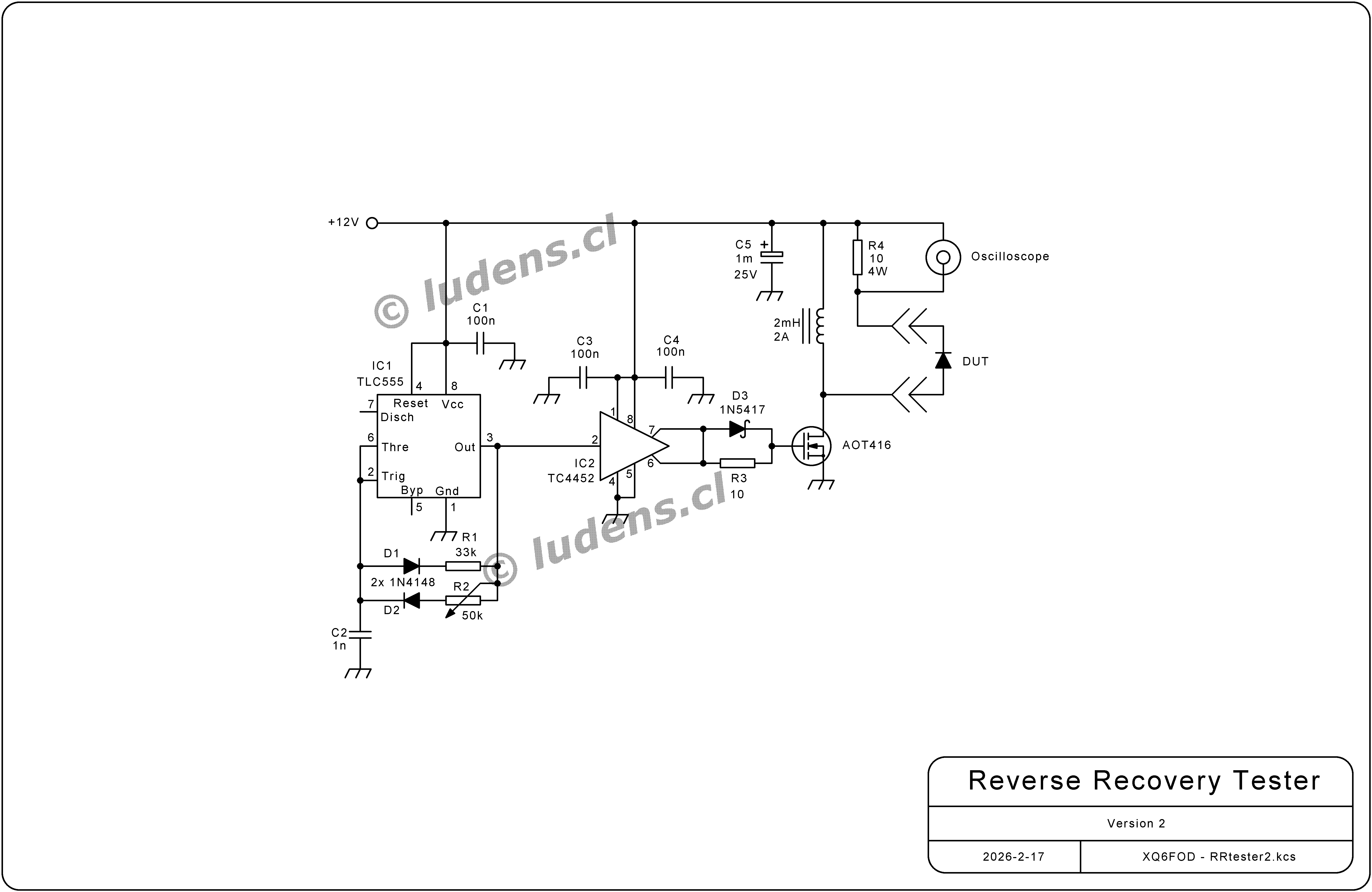
 As
usual on my site, you can click this schematic to get a high-resolution
version for printing.
As
usual on my site, you can click this schematic to get a high-resolution
version for printing.
A
CMOS 555 timer IC is used to generate a pulse signal having
an ON
time adjustable by R2 from roughly 1.5 to 35µs, while the OFF time is
fixed at about 25µs. This pulse goes through a relatively fast and
powerful gate driver IC, which drives a MOSFET with the fastest
possible turn-on time, while the turn-off time is allowed to
be a
little slower, mainly to get some resistive damping into the gate
circuit.
The MOSFET drives an inductive/resistive circuit around
the diode to be tested. The use of an inductor allows running the
circuit from a single supply, that doesn't need to deliver as much
current as used to forward-bias the diode. An oscilloscope is used to
measure the voltage drop on the resistor in series with the diode, to
get a display of the diode current. Note that the positive side of the
power supply connects to the "ground" of the scope probe. So, if the
scope and its probe are actually grounded, a floating power supply is
needed. Most lab power supplies deliver floating output, so that's no
problem. A grounded +/- supply can also be used, by using
its negative side.
While the MOSFET is on, the
inductor current slowly increases, storing energy in the magnetic
field. When the MOSFET is off, the inductor current flows through the
diode under test and R4. The inductor's value is large enough to keep
the current reasonably constant over the whole period. By adjusting R2
to the proper pulse width, one can precisely set the forward current in
the diode just before the MOSFET turns on. At the moment the MOSFET
does turns on, it not only begins to conduct the inductor's current,
but also reverse-biases the diode, and conducts its reverse recovery
current. This current is limited mainly by the supply voltage and
the value of R4, so that by choosing the value of R4 it is possible to
set
the desired reverse current limit, and the value can be fine-tuned by
varying the supply voltage. The circuit will work correctly with supply
voltages from 10 to 15V, giving enough range for this fine setting of
the reverse current.
When building the circuit, there are two
circuit loops with should be kept as short and direct as possible. One
is the loop formed IC2, D3, the MOSFET, ground return to IC2, and C3
and C4. This must be short in order to assure the fastest possible
turn-on of the MOSFET. The other circuit that needs low stray
inductance (thus short connections) is the one formed by the diode
under test with R4, C5 and the MOSFET. Instead the inductor doesn't
need short terminals. Any stray inductance in its connections
simply ads to its main inductance.
The 555 timer should be
the CMOS version (TLC555), because the standard version is too slow,
and can't create short enough pulses. The TC4452 driver can be replaced
by weaker or slower drivers, such as the TC4420 or TC4422, at a slight
loss of MOSFET turn-on speed. Since manufacturers use pretty fast pulse
generators to test their diodes for reverse recovery, it's good to have
fast turn-on here, to get a reasonable match of measured values with
datasheet numbers. So, if you can, use a fast and powerful driver IC.
The MOSFET I chose is the best suited one
from among the ones I had within easy reach in my lab when assembling
this circuit. It can be replaced by many different MOSFETs. If you do
so, try to find a MOSFET that has a low gate charge and low
capacitances. That's more important than a super low RDSon, in this
application. When measuring with a 10Ω sensing resistor, an RDSon as
high as a few hundred milliohm is acceptable.
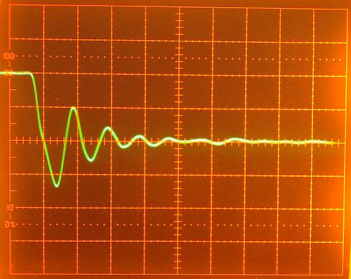
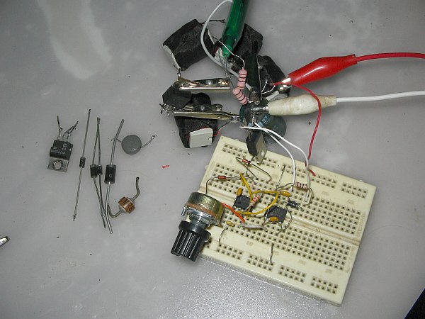 As
happens so often nowadays, I was too lazy to build the circuit in a
decent way, and instead assembled the small-signal part on a small
protoboard, with 3D-construction of the power circuit. My MOSFET drive
and ground return connections are longer than optimal, but it works
well enough for these tests, even if it causes some ringing.
As
happens so often nowadays, I was too lazy to build the circuit in a
decent way, and instead assembled the small-signal part on a small
protoboard, with 3D-construction of the power circuit. My MOSFET drive
and ground return connections are longer than optimal, but it works
well enough for these tests, even if it causes some ringing.
Since this is just a quick-and-dirty circuit, I used four 470µH
inductors in series, instead of a nice single 2mH one. I had them lying
around on my workbench, from playing with speaker crossovers. These are
inductors wound with wire about 1mm thick, on chunky ferrite solenoids.
The green ballpen is my homemade Z0 scope probe. Of course the ballpen
had its guts replaced. Ink tube and ball point went out, voltage
divider resistor went in. Z0 probes work better than any affordable
high impedance probes, when fast response is needed.
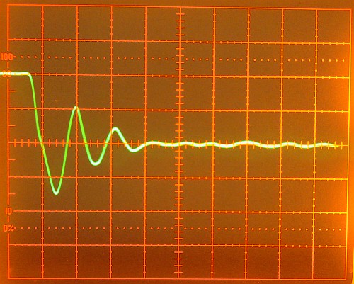
For quick-and-dirty measurement, I clamped the diode under test in the
alligator clips. The alligators provide electrical connection and some
heat dissipation.
The circuit has two resistors for R4. I can quickly connect
one, the other, or both in parallel.
It would be easy to build this circuit in a permanent way, with a
selection of different resistor values for R4, but the question is
whether it will be really useful! I have been doing electronics for 45
years
now, and this is the first time I actually needed to measure the
reverse
recovery of a diode, instead of just trusting the datasheets. How often
will I do it in the future? Maybe never.
So, let's go to what I measured with this contraption.
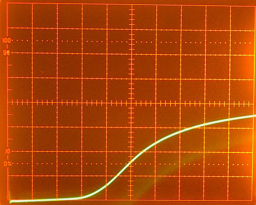
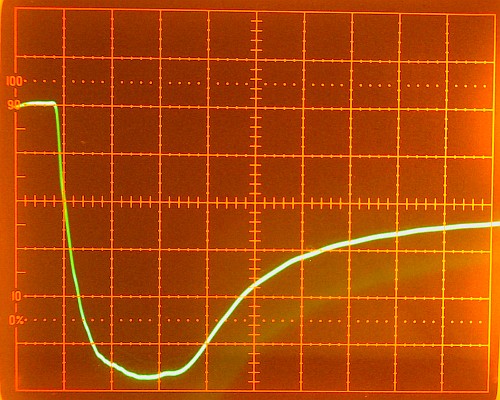
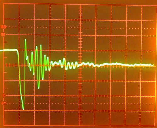
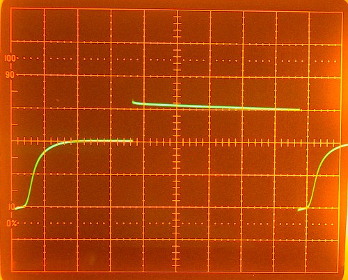 Here
is an oscillogram showing the complete waveform on R4. Scale is 0.5A
per division vertically with zero at the center line, and 5µs
per
division horizontally.
Here
is an oscillogram showing the complete waveform on R4. Scale is 0.5A
per division vertically with zero at the center line, and 5µs
per
division horizontally.
The trigger is set to the falling
edge at the moment the MOSFET turns on. The current goes very quickly
to -1A, and stays there for roughly 2µs. Then the diode can no longer
conduct all that reverse current, and the trace shows a very soft diode
recovery. It crosses the level of -0.25A roughly at 4µs, so this would
be the reverse recovery time rating of this diode, a 1N5406.
Then
the reverse current decays to zero, while the inductor is charging its
field. At 18µs the MOSFET stops conducting, so that the inductor begins
dumping its current into the diode. At first we have about 0.6A of
forward current, which slowly decays to 0.5A at about 44µs, when the
MOSFET turns on again, and the cycle begins to repeat.
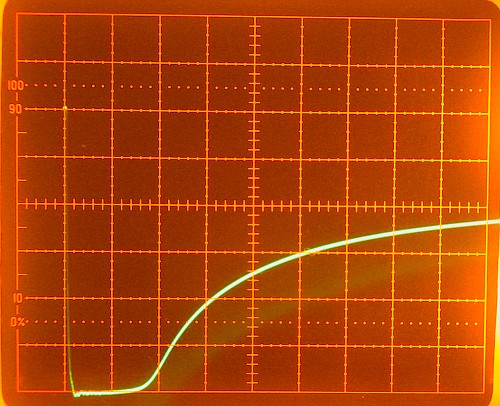
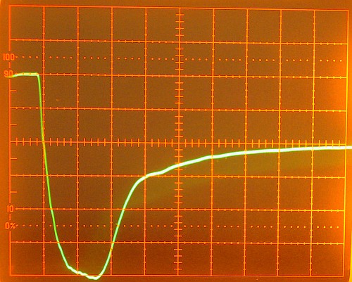
 For
a practical measurement, of course we should zoom in on the interesting
part of the curve, to get better resolution. So here we have the
reverse recovery area of the same measurement, but at a scale of 0.25A
and 0.5µs per division.
For
a practical measurement, of course we should zoom in on the interesting
part of the curve, to get better resolution. So here we have the
reverse recovery area of the same measurement, but at a scale of 0.25A
and 0.5µs per division.
There is just a little dot of the 0.5A
forward current visible, inside the zero of the 90% marking on the
screen. It is now possible to determine the -0.25A point much more
precisely: It happens at 3.7µs. So that's the precisely measured
reverse recovery time of this diode. It's a standard rectifier,
optimized for low voltage drop, not for high recovery speed. The two
parameters are tied: When the manufacturer speeds up a diode, by
shortening the carrier lifetime, the forward voltage drop gets larger.
 Now
let's compare several diodes rated at 1A. I will keep the vertical
scale fixed at 0.25A per division, but set the time scale so that each
diode can be measured with good accuracy. I also now set the horizontal
shift control so that the current zero crossing happens one division in
from the left, for more accurate measurement of the timing.
Now
let's compare several diodes rated at 1A. I will keep the vertical
scale fixed at 0.25A per division, but set the time scale so that each
diode can be measured with good accuracy. I also now set the horizontal
shift control so that the current zero crossing happens one division in
from the left, for more accurate measurement of the timing.
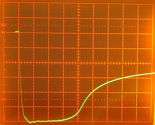
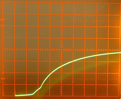
This
is a 1N4007, very well known to any electronician. The time scale is
200ns/div. As you can see, after having been conducting 0.5A forward
current, it will conduct my circuit-limited -1A of reverse current for
about 300ns, then the current will decrease, and cross -0.25A at a tiny
little bit more than 1µs. So it's fair to say that this particular
diode has a reverse recovery time of 1µs, which is on the fast side for
a high-voltage standard rectifier.
The datasheets of standard recovery diodes
usually don't mention the reverse recovery time, because it's
irrelevant for line-frequency operation, and that's what these diodes
are made for. It can vary quite a lot for identically marked diodes
made by different companies, or even per batch.
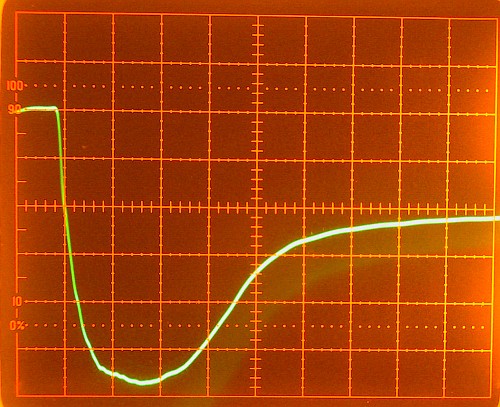
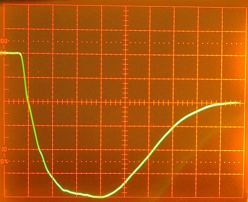
 This
is a vintage, pancake-shape SD-1 diode, dating from the early 1960s,
rated at 1A and 600V. The time scale is 50ns/div. The reverse recovery
time is 350ns, making this a "fast" rectifier. Not bad, for that time!
This
is a vintage, pancake-shape SD-1 diode, dating from the early 1960s,
rated at 1A and 600V. The time scale is 50ns/div. The reverse recovery
time is 350ns, making this a "fast" rectifier. Not bad, for that time!
 This
is a true UF4007, an ultrafast 1A, 1000V diode. I had to change the
time scale to 20ns/div. The limited slew rate of my MOSFET and driver
are now easily visible.
This
is a true UF4007, an ultrafast 1A, 1000V diode. I had to change the
time scale to 20ns/div. The limited slew rate of my MOSFET and driver
are now easily visible.
The diode barely even reaches -1A of
reverse current. It's so fast that by the time my MOSFET is fully on,
the diode is already so far recovered that it begins to limit the
current.
The -0.25A crossing happens roughly 85ns after the
downgoing zero crossing. So that's the measured recovery time. The
datasheet for this diode claims 75ns, but that's valid at 25°C! The
manufacturers measure this by subjecting a cold diode to a single
pulse. It's one of many tricks they use to make products appear better
than they are! Because in practical use, rectifying 0.5A, obviously a
diode will be quite warm, and the reverse recovery time gets worse at
higher temperature.
My test circuit subjects the
diodes to an average current that is comparable to what it
would
see in a typical real switching power supply, so my test result is more
realistic than what the datasheet promises.
 This is the Chinese
UF4007. The scaling is the same as above. The
reverse recovery time is roughly 110ns, because the diode runs
extremely hot, due to the inadequate thermal conductivity of its very
thin pins.
This is the Chinese
UF4007. The scaling is the same as above. The
reverse recovery time is roughly 110ns, because the diode runs
extremely hot, due to the inadequate thermal conductivity of its very
thin pins.
It's so much fun to watch the reverse recovery time of this diode
degrade as it warms up, that I made a short video
of it! There you can see the reverse recovery time of this diode
starting at 60ns when cold, and degrading to more than 100ns
in a
matter of 20 seconds of warming up. Never mind the autoexposure of my
webcam playing crazy at the beginning...
 Schottky
diodes are the fastest kids on the block, way faster than "ultrafast"
ones! Being majority-carrier devices, their recovery time is so fast
that it tends to get masked by the ringing, and for this reason
manufacturers often say that these diodes don't have a reverse recovery
at all.
Schottky
diodes are the fastest kids on the block, way faster than "ultrafast"
ones! Being majority-carrier devices, their recovery time is so fast
that it tends to get masked by the ringing, and for this reason
manufacturers often say that these diodes don't have a reverse recovery
at all.
This image shows the behavior of an MBR160 Schottky
diode. The time scale is 10ns/div. Indeed no reverse conduction can be
seen, instead there is strong ringing at a frequency of
roughly
100MHz. The resonant frequency is given mainly by the junction
capacitance of the diode and the stray inductance of the loop formed by
the diode, MOSFET, C5 and R4. This inductance is roughly 70nH in my
3D-built circuit, while the junction capacitance of this diode is
roughly 40pF at the reverse voltage of about 10V that my circuit
applies.
Schottky diodes have much larger capacitances
than PN diodes of the same size. For example, the UF4001,
which is
comparable to the MBR160 in current and voltage rating, only has about
15pF at 10V.
 This
is another, very similar Schottky diode, a 1N5817. The
ringing is
a little stronger, and its frequency is a little lower, indicating even
higher junction capacitance. According to the datasheet, it's 55pF at
10V. No surprise there.
This
is another, very similar Schottky diode, a 1N5817. The
ringing is
a little stronger, and its frequency is a little lower, indicating even
higher junction capacitance. According to the datasheet, it's 55pF at
10V. No surprise there.
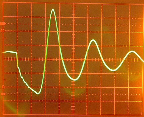
 Let's
look at diodes of other sizes. This is an MR821, a pretty old, fast
rectifier rated at 5A and 100V. The time scale is 20ns/div. The
measured recovery time is a very respectable 60ns.
Let's
look at diodes of other sizes. This is an MR821, a pretty old, fast
rectifier rated at 5A and 100V. The time scale is 20ns/div. The
measured recovery time is a very respectable 60ns.
 Now
it gets interesting! This is an RF diode, the well-known 1N4148, rated
at 100mA and 100V. The time scale is 10ns/div, and I also changed the
vertical scale to 100mA/div. I set a forward current of 100mA, even if
the datasheet gives a reverse recovery time measurement done at only
10mA forward current, and just 1mA reverse current! That might actually
be a typo. In any case, my MOSFET and driver are too slow to
reach a high reverse current peak before the diode recovers, but the
reverse current peaks at -300mA, and the recovery time measures 4ns,
which happens to match perfectly with the value given in the datasheet
for different conditions! That coincidence was sheer luck.
Now
it gets interesting! This is an RF diode, the well-known 1N4148, rated
at 100mA and 100V. The time scale is 10ns/div, and I also changed the
vertical scale to 100mA/div. I set a forward current of 100mA, even if
the datasheet gives a reverse recovery time measurement done at only
10mA forward current, and just 1mA reverse current! That might actually
be a typo. In any case, my MOSFET and driver are too slow to
reach a high reverse current peak before the diode recovers, but the
reverse current peaks at -300mA, and the recovery time measures 4ns,
which happens to match perfectly with the value given in the datasheet
for different conditions! That coincidence was sheer luck.
After the diode recovers, there is a
lot of ringing, looking rather adventurous. This is triggered by the
very hard recovery characteristic of this diode.Since this diode has a
much lower capacitance, the main ringing frequency is roughly 400MHz.
The
oscilloscope and test probe must be fast ones, to measure such diodes.
Mine is a Tektronix 485, with a homemade Z0 probe. The combination
delivers a risetime barely over 1ns.
The next step would be
measuring a small-signal Schottky diode, like the 1N5711, which has a
rated reverse recovery time of 100 picoseconds. But that would not only
require a much faster pulse generator, but also a
$100,000 oscilloscope! I prefer to test the speed of such
diodes
with an RF signal generator, testing at what frequency their
rectification efficiency falls off.
 Let's
go to very big and very slow diodes instead: The body diodes of
MOSFETs. It's easy to disable a MOSFET by shorting its gate to its
source, and then one can measure the body diode just like any
stand-alone diode.
Let's
go to very big and very slow diodes instead: The body diodes of
MOSFETs. It's easy to disable a MOSFET by shorting its gate to its
source, and then one can measure the body diode just like any
stand-alone diode.
This image shows the result obtained from a
rather old 2SK1120 MOSFET, rated at 1000V, 8A, with an RDSon of 1.5Ω.
The time scale is 1µs/div, and the vertical scale has been returned to
0.25A/div. The forward current used is again 0.5A, barely visible as a
tiny spot. The
reverse recovery time of this MOSFET's body diode is a horrible 5µs!
It
goes without saying that a MOSFET with such a slow diode recovery
cannot be used in switching power supplies where the body diodes are
part of the game, such as in bridge circuits. But it's fine to use in
circuits that don't turn the body diode on, such as boost converters,
fly-back converters,
or in very -slow-switching circuits.
 Low-voltage
MOSFETs generally have very much faster body diodes than high-voltage
ones. Modern MOSFETs are usually much better than old ones, and on top
of that a manufacturer can put more or less emphasis on speeding up the
body diode, depending on the intended application range of a specific
MOSFET. Improving the diode recovery speed will always worsen some
other
parameters.
Low-voltage
MOSFETs generally have very much faster body diodes than high-voltage
ones. Modern MOSFETs are usually much better than old ones, and on top
of that a manufacturer can put more or less emphasis on speeding up the
body diode, depending on the intended application range of a specific
MOSFET. Improving the diode recovery speed will always worsen some
other
parameters.
This image shows the recovery of the body diode of
an IRF3205, a 55V, 110A, 8mΩ MOSFET very often used in
inverters
for 12V battery systems. The time scale is 10ns/div, and the measured
reverse
recovery time is barely 60ns! So the body diode of this MOSFET has a
recovery time like an ultrafast rectifier! It can be used as a circuit
element, if needed, but still Schottky diodes are better.
The
datasheet states a reverse recovery time of 69ns, even if under totally
different conditions than my circuit sets: 62A forward current, no
fixed reverse current limit, but a 100A/µs slew rate limit on the
current. My circuit was set to apply just 0.5A of forward current, but
the current slew rate is also 100A/µs, which can be seen by the rate of
rise of reverse current just after the current zero crossing: 0.5A in
5ns, which equals 100A/µs. The recovery time of a diode does not depend
very much on the absolute currents, but instead on the ratio
between forward and reverse current. If the di/dt of a testing system
is fixed, then at any forward test current the same ratio of forward to
peak reverse current will result, and this should give about the same
recovery time.
 To
test with higher currents, I replaced R4 by a 1Ω
resistor.
Well, it didn't come out as nicely as intended... But it's still
usable, and interesting! This is the IRF3205 with R4 changed to 1Ω. I
set the vertical scale to 2A/div, the time scale to 20ns/div,
and
the forward current to 1A. What happens now is that with so little
resistive damping, and the higher reverse current (peaking at -5A), the
ringing became big, dominating the picture. This is made even much
worse by the low value of the resistor making its own inductance a big
factor, making the oscilloscope giving an exaggerated high-frequency
response.
To
test with higher currents, I replaced R4 by a 1Ω
resistor.
Well, it didn't come out as nicely as intended... But it's still
usable, and interesting! This is the IRF3205 with R4 changed to 1Ω. I
set the vertical scale to 2A/div, the time scale to 20ns/div,
and
the forward current to 1A. What happens now is that with so little
resistive damping, and the higher reverse current (peaking at -5A), the
ringing became big, dominating the picture. This is made even much
worse by the low value of the resistor making its own inductance a big
factor, making the oscilloscope giving an exaggerated high-frequency
response.
The average di/dt is now roughly 150A/µs, 50% higher
than the one used by the manufacturer for testing, and looks like a
sine section rather than a ramp, because the current is being defined
by the stray inductance and parts capacitance, more than by resistance.
Under these conditions, the reverse recovery time comes
out just
under 40ns, significantly faster than the 69ns stated in the datasheet
as typical value.
If you paid attention, you will have noticed
that the measured recovery time tends to be inversely proportional to
the di/dt
provided by the test circuit!
All this playing
shines a lot of light into the often obscure reverse recovery ratings.
An important point to take home is this: A diode does not have a
specific reverse recovery time. It's nonsense to say "this diode
recovers in 50ns". Instead it's essential to state under what set of
conditions a certain recovery time was measured, and the manufacturers
do so. The problem is that different diodes are rated under different
conditions, and then the published recovery times cannot be directly
compared. When having the diodes at hand, a simple test circuit like
this one can be used to quickly compare diodes under identical
conditions.
Maybe it would be best to specify the
recovery of diodes by two numbers: The total charge stored in
the
junction per ampere of forward current, and the charge carrier half
life. When a diode conducts forward current, and then the current is
stopped, the charge in the junction will slowly disappear on its own,
by recombination. If instead a diode that was conducting is quickly
switched to reverse polarity, most of the charge is drained out by
reverse current, and natural recombination plays almost no role. If the
application circuit limits the reverse current to a modest value, then
both charge removal and recombination will take part in the process. By
having data for the carrier half life, and the total charge per
current, the recovery behavior of a diode is better described
than
by a single recovery time spec under a specific set of conditions.
The
pulse generator and driver can be used for various different power
circuits. Feel free to modify, test and play! If you want to test
really large diodes, it will become necessary to use a MOSFET with low
enough RDSon, high enough voltage rating, change the values of the
inductor, R4 and C5, and use two separate power supplies: A
small
12V one to power the ICs, and a higher voltage, sufficiently powerful
one for the power circuit. When using a low value for R4, it would be
best to build it from several SMDs in parallel, and use an RC
compensation network to remove the high-frequency peaking caused by
what little inductance the sensing resistor still has. It's also
possible to eliminate the inductor, and use the pulse generator with
two power supplies and several power resistors to make the kind of test
circuit often detailed in diode datasheets.
As shown in the
diagram, my circuit is very well suited to do the typical testing of
small and medium diodes used in switching power supplies, which are
usually tested by the manufacturers at 0.5A forward current
and 1A
reverse current.
Back to homo ludens
electronicus.